photodetector - sugito.staff.telkomuniversity.ac.id · dibawah tegangan breakdown jumlah carrier yg...
TRANSCRIPT
Fakultas Teknik Elektro 1
PHOTODETECTOR
Ref : Keiser
Fakultas Teknik Elektro 2
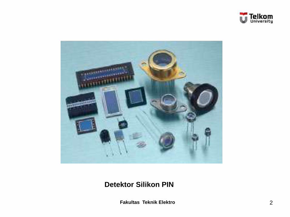
Detektor Silikon PIN
Fakultas Teknik Elektro 3
Syarat foto detektor
• High response atau sensitifitas
• Noise rendah
• Respon cepat atau bandwidth lebar
• Tidak sensitif thd variasi suhu
• Kompatibel dgn fiber
• Murah
• Tahan lama
Fakultas Teknik Elektro 4
Detektor foto yg ada
• Photomultiplier (photocathode + multiplier
dlm vacum tube)
• Pyroelectric detector (konversi photon ke
panas konstanta dielektrik)
• Semiconductor-based photoconductor
(pin dan APD) cocok u fiber optik.

Fakultas Teknik Elektro 5
Fakultas Teknik Elektro 6
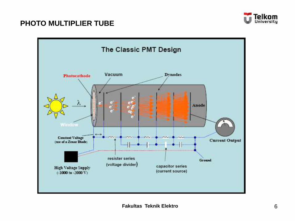
PHOTO MULTIPLIER TUBE
Fakultas Teknik Elektro 7
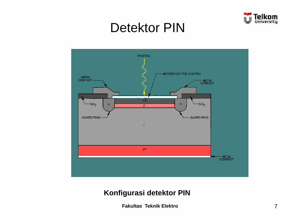
Konfigurasi detektor PIN
Detektor PIN
Fakultas Teknik Elektro 8
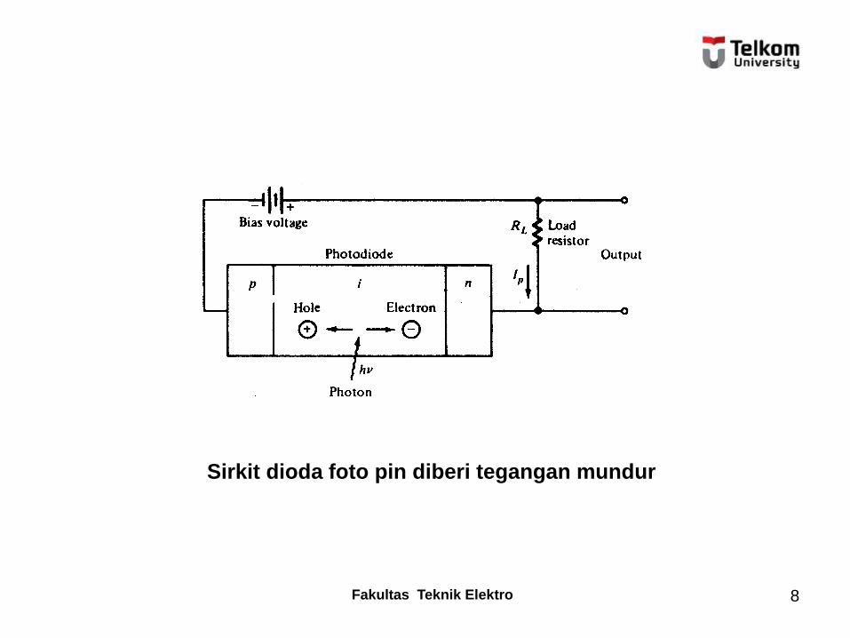
Sirkit dioda foto pin diberi tegangan mundur
Fakultas Teknik Elektro 9
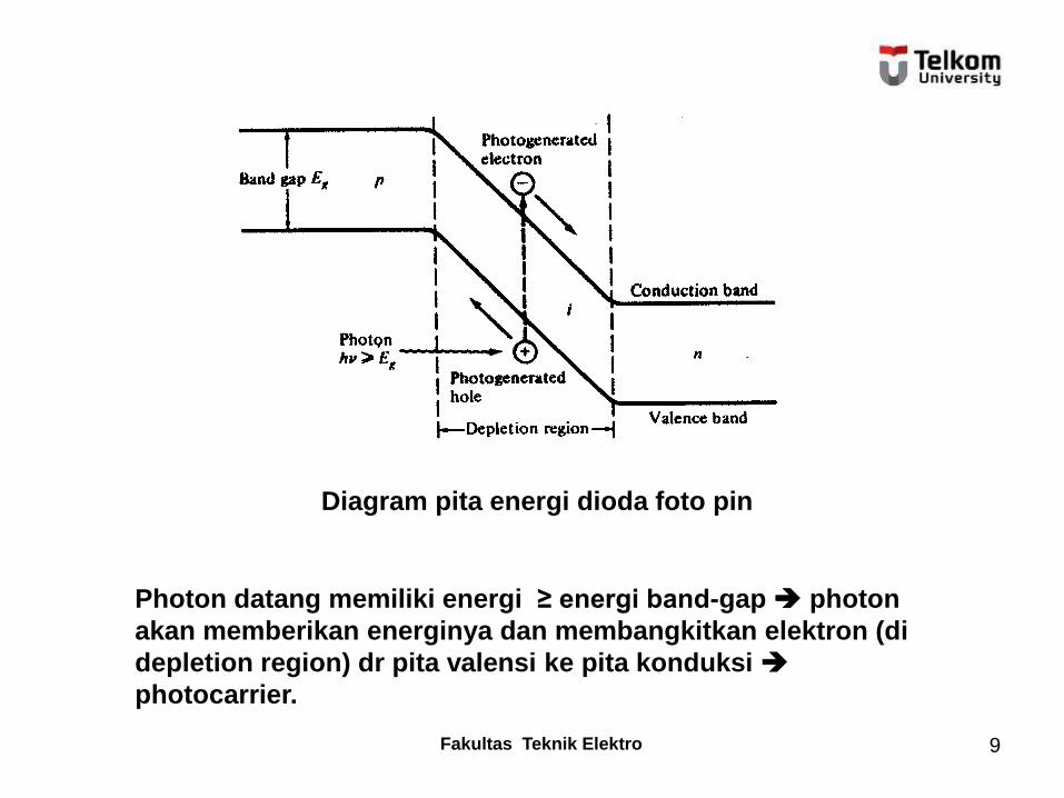
Photon datang memiliki energi ≥ energi band-gap photon
akan memberikan energinya dan membangkitkan elektron (di
depletion region) dr pita valensi ke pita konduksi
photocarrier.
Diagram pita energi dioda foto pin

Fakultas Teknik Elektro 10
ppp
nnn
DL
DL
Dn : koefisien difusi elektron
Dp : koefisien difusi hole
Carrier bermuatan mengalir melalui material, beberapa
pasangan elektron-hole berekombinasi dan hilang.
Elektron bergerak sejauh Ln sedang hole bergerak
sejauh Lp.
Jarak tsb disebut panjang difusi.
Waktu yg dibutuhkan berekombinasi disebut carrier
lifetime, elektron selama n dan hole selama p.
Fakultas Teknik Elektro 11
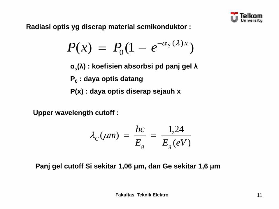
Radiasi optis yg diserap material semikonduktor :
)1()()(
0
xSePxP
αs(λ) : koefisien absorbsi pd panj gel λ
P0 : daya optis datang
P(x) : daya optis diserap sejauh x
Upper wavelength cutoff :
)(
24,1)(
eVEE
hcm
gg
C
Panj gel cutoff Si sekitar 1,06 μm, dan Ge sekitar 1,6 μm
Fakultas Teknik Elektro 12
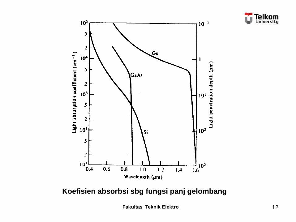
Koefisien absorbsi sbg fungsi panj gelombang
Fakultas Teknik Elektro 13
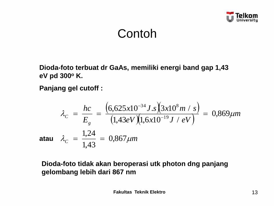
Contoh
Dioda-foto terbuat dr GaAs, memiliki energi band gap 1,43
eV pd 300o K.
Panjang gel cutoff :
m
meVJxeV
smxsJx
E
hc
C
g
C
867,043,1
24,1
869,0/106,143,1
/103.10625,619
834
atau
Dioda-foto tidak akan beroperasi utk photon dng panjang
gelombang lebih dari 867 nm
Fakultas Teknik Elektro 14
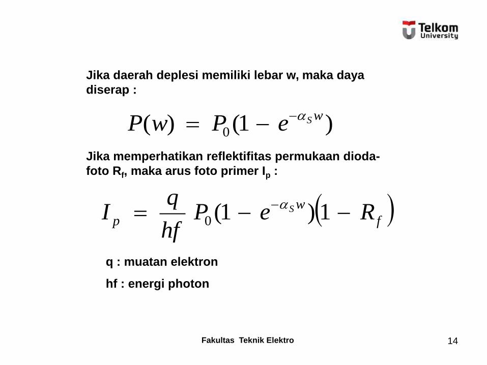
Jika daerah deplesi memiliki lebar w, maka daya
diserap :
)1()( 0
wSePwP
Jika memperhatikan reflektifitas permukaan dioda-
foto Rf, maka arus foto primer Ip :
f
w
p RePhf
qI S
1)1(0
q : muatan elektron
hf : energi photon
Fakultas Teknik Elektro 15
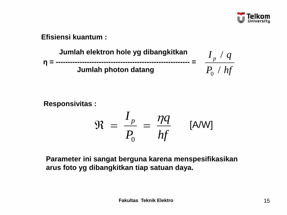
Efisiensi kuantum :
Jumlah elektron hole yg dibangkitkan
η = -------------------------------------------------------- = Jumlah photon datang hfP
qI p
/
/
0
Responsivitas :
hf
q
P
I p
0
Parameter ini sangat berguna karena menspesifikasikan
arus foto yg dibangkitkan tiap satuan daya.
[A/W]
Fakultas Teknik Elektro 16
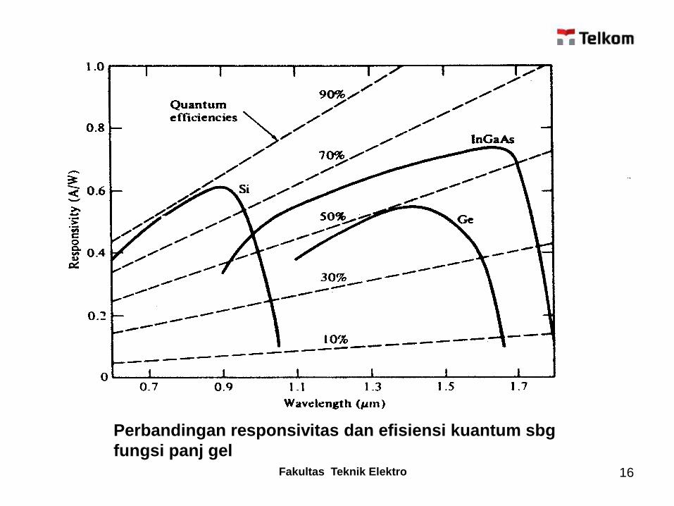
Perbandingan responsivitas dan efisiensi kuantum sbg
fungsi panj gel
Fakultas Teknik Elektro 17
Contoh
InGaAs pd panj gel 1100 nm < λ < 1600 nm, memiliki
efisiensi kuantum 60 %.
Berapa responsivitasnya pd panj gel 1300 nm ?
Jika daya optis yg datang 10 μW, berapa arus foton yg
dibangkitkan ?

Fakultas Teknik Elektro 18
Avalanche Photodiode (APD)
Fakultas Teknik Elektro 19
Avalanche Photodiode
APD secara internal melipat gandakan arus foto sinyal
primer sebelum memasuki sirkit penguat
meningkatkan sensitifitas penerima.
Mekanisme pelipatgandaan elektron/hole disebut
impact ionization.
Carrier baru yg dibangkitkan juga dipercepat oleh
medan listrik kuat, shg menguatkan energi utk impact
ionization selanjutnya.
Phenomena tsb disebut efek avalanche.
Dibawah tegangan breakdown jumlah carrier yg
dibangkitkan tertentu, sedangkan diatas tegangan
breakdown carrier yg dibangkitkan dpt tak terbatas.
Fakultas Teknik Elektro 20
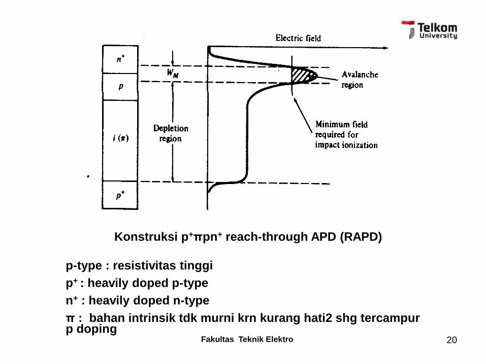
Konstruksi p+πpn+ reach-through APD (RAPD)
p-type : resistivitas tinggi
p+ : heavily doped p-type
n+ : heavily doped n-type
π : bahan intrinsik tdk murni krn kurang hati2 shg tercampur p doping
Fakultas Teknik Elektro
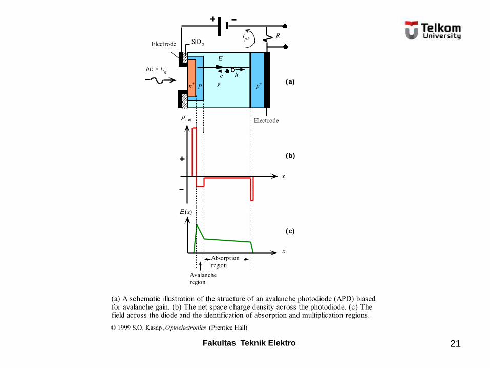
š p+
SiO2Electrode
net
x
x
E(x)
R
E
h > Eg
p
Ip h
e– h+
Absorption
region
Avalanche
region
(a)
(b)
(c)
(a) A schematic illustration of the structure of an avalanche photodiode (APD) biasedfor avalanche gain. (b) The net space charge density across the photodiode. (c) Thefield across the diode and the identification of absorption and multiplication regions.
Electrode
© 1999 S.O. Kasap, Optoelectronics (Prentice Hall)
n+
21

Fakultas Teknik Elektro
h+
E
šn+ p
e–
Avalanche region
e–
h+
Ec
Ev
(a) (b)
E
(a) A pictorial view of impact ionization processes releasing EHPs andthe resulting avalanche multiplication. (b) Impact of an energeticconduction electron with crystal vibrations transfers the electron'skinetic energy to a valence electron and thereby excites it to theconduction band.
© 1999 S.O. Kasap, Optoelectronics (Prentice Hall)
22
EHP : Electron Hole Pair
Fakultas Teknik Elektro
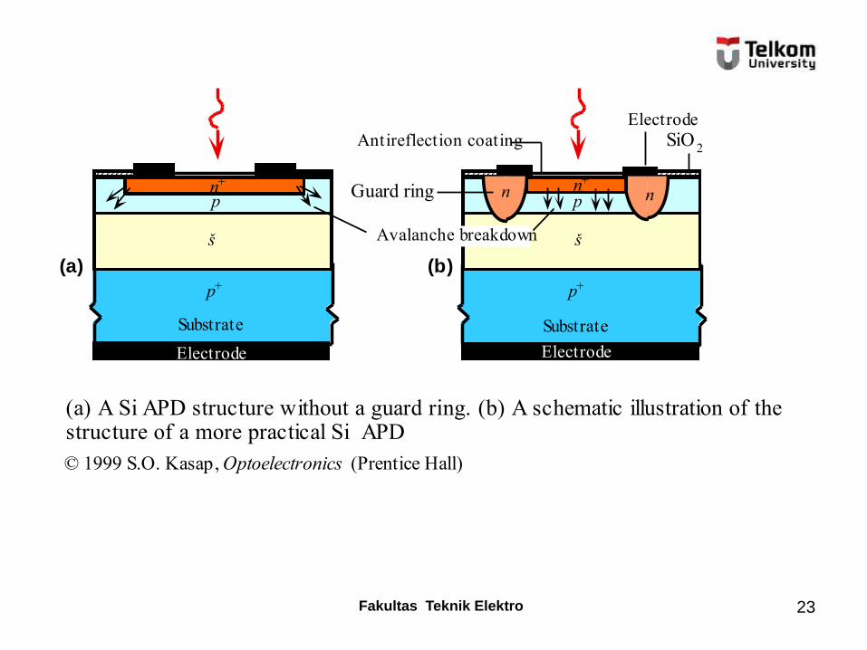
SiO2
Guard ring
Electrode
Antireflection coating
nn n+
p+
š
p
Substrate
Electrode
n+
p+
š
p
Substrate
Electrode
Avalanche breakdown
(a) (b)
(a) A Si APD structure without a guard ring. (b) A schematic illustration of thestructure of a more practical Si APD
© 1999 S.O. Kasap, Optoelectronics (Prentice Hall)
23

Fakultas Teknik Elektro
E
N n
Electrode
x
E(x)
R
h
Iph
Absorption
region
Avalanche
region
InP InGaAs
h+
e–E
InP
P+ n+
Simplified schematic diagram of a separat e absorpt ion and multiplicat ion(SAM) APD using a heterostructure based on InGaAs-InP. P and N refer t op and n -t ype wider-bandgap semiconductor.
Vr
Vout
© 1999 S.O. Kasap, Optoelectronics (Prentice Hall)
24

Fakultas Teknik Elektro 25
Pd penggunaan normal RAPD bekerja pd modus depleted
penuh.
Cahaya memasuki device mel daerah p+ dan diserap bahan
π yg bekerja sbg daerah pengumpul carrier yg dibangkitkan
oleh photon.
Saat diserap photon memberikan energi, shg
membangkitkan pasangan elektron-hole yg
kemudiandipisahkan oleh medan listrik di daerah π.
Elektron yg dibangkitkan oleh photon bergeser dr daerah π
ke pn+ junction yg terdapat medan listrik kuat.
Pd daerah medan listrik kuat terjadi pelipat gandaan carrier.
Fakultas Teknik Elektro 26
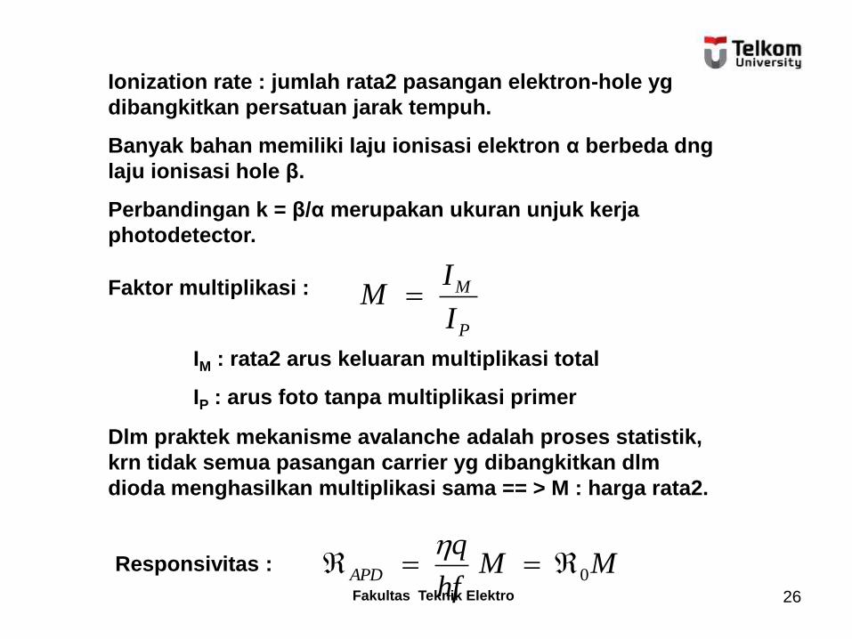
Ionization rate : jumlah rata2 pasangan elektron-hole yg
dibangkitkan persatuan jarak tempuh.
Banyak bahan memiliki laju ionisasi elektron α berbeda dng
laju ionisasi hole β.
Perbandingan k = β/α merupakan ukuran unjuk kerja
photodetector.
Faktor multiplikasi :
P
M
I
IM
IM : rata2 arus keluaran multiplikasi total
IP : arus foto tanpa multiplikasi primer
Dlm praktek mekanisme avalanche adalah proses statistik,
krn tidak semua pasangan carrier yg dibangkitkan dlm
dioda menghasilkan multiplikasi sama == > M : harga rata2.
Responsivitas : MMhf
qAPD 0
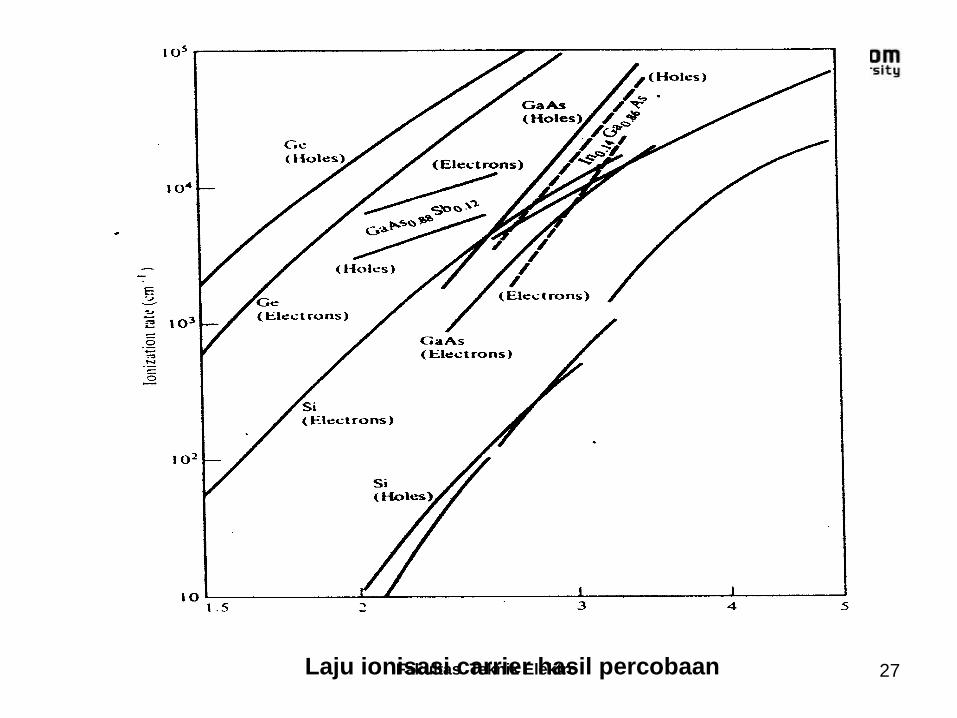
Fakultas Teknik Elektro 27Laju ionisasi carrier hasil percobaan
Fakultas Teknik Elektro 28
Contoh
Suatu APD memiliki efisiensi kuantum 65 % pd panj gel
900 nm. Jika daya optis 0,50 μW menghasilkan arus foto
multiplikasi 10 μA, berapa faktor multiplikasi M ?
Fakultas Teknik Elektro 29
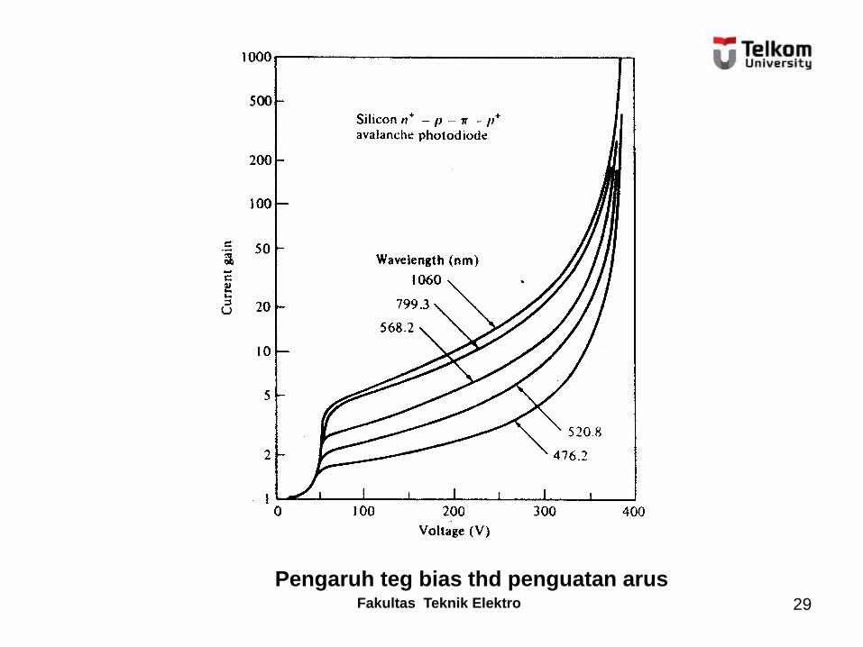
Pengaruh teg bias thd penguatan arus
Fakultas Teknik Elektro 30
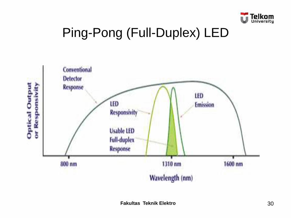
Ping-Pong (Full-Duplex) LED