semikonduktor - bakada2014.files.wordpress.com · a donor atom, such as phosphorus, has five...
TRANSCRIPT

SEMIKONDUKTOR
Bahan yang mempunyai sifat listrik diantara konduktor dan isolator
Bahan semikonduktor dibagi menjadi dua : Intrisik (murni):Semi konduktor tidak ada cacat kisi danpengotor dalam kristalnya. Sifat listriknya ditentukanoleh bahan itu sendiriEkstrisik (tak murni): Adanya impuritas/cacat kisisehingga sifat listriknya ditentunkan oleh rekayasamanusia.
Berdasarkan teori pita energy dibagi menjadi dua jenis:Direct semikonduktorIndirect semikonduktor

Transisi elektron langsung (direct)
k=vektor gelombang
Et : tingkat energi cacat/transisi
Transisi elektron tak langsung
(indirect)

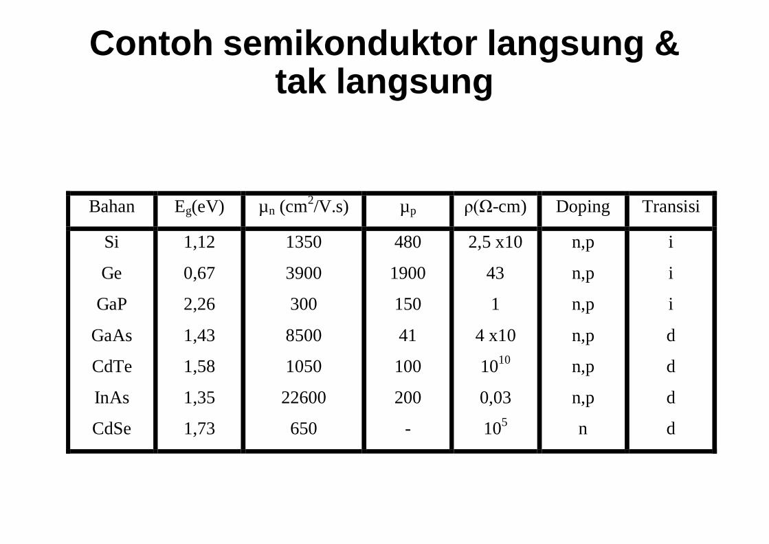
Contoh semikonduktor langsung & tak langsung
Bahan Eg(eV) µn (cm2/V.s) µp ρ(Ω-cm) Doping Transisi
Si
Ge
GaP
GaAs
CdTe
InAs
CdSe
1,12
0,67
2,26
1,43
1,58
1,35
1,73
1350
3900
300
8500
1050
22600
650
480
1900
150
41
100
200
-
2,5 x10
43
1
4 x10
1010
0,03
105
n,p
n,p
n,p
n,p
n,p
n,p
n
i
i
i
d
d
d
d

Bahan SemikonduktorSemiconductor materials: Elemental semiconductors: Si, Ge III-V compounds: AlP, AlAs, GaN, GaP, GaAs, InAs, InP II-VI compounds: ZnO, ZnSe, ZnTe, CdS, CdSe, CdTe Alloys: AlxGa1-xAs, GaxIn1-xAs1-yPy
The spatial arrangement of atoms within a material plays an important role in determining the precise properties of the material. Based on the degree of atomic order, materials can be classified as: Amorphous => no recognizable long-range order Polycrystalline => completely ordered in segments Crystalline => Entire solid is made up of atoms in an orderly array

Candidate Materials Group III-V & Group II-VI
iviii v
ii
Periodic Table to show group III-V and II-V binaries
Group II Group III Group IV Group V
Al
Ga
In
N
P
As
with a tetra-hedral unit cell.
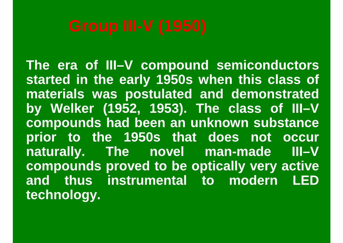
Group III-V (1950)
The era of III–V compound semiconductorsstarted in the early 1950s when this class ofmaterials was postulated and demonstratedby Welker (1952, 1953). The class of III–Vcompounds had been an unknown substanceprior to the 1950s that does not occurnaturally. The novel man-made III–Vcompounds proved to be optically very activeand thus instrumental to modern LEDtechnology.

Group III-V LED materials
Al
Ga
In
N
P
As
AlN, AlP,AlAs
GaN, GaP, GaAs
InN, InP, InAs
GaAs GaP
GaAl
GaAsP
GaAsAl
Questions to ask when choosing the right material:1. Can it be doped or not?
2. What wavelength it can emit?3. Would the material able to allow radiative recombiation?
4. Direct or indirect semiconductor?
Ternarycompounds
Binary compounds
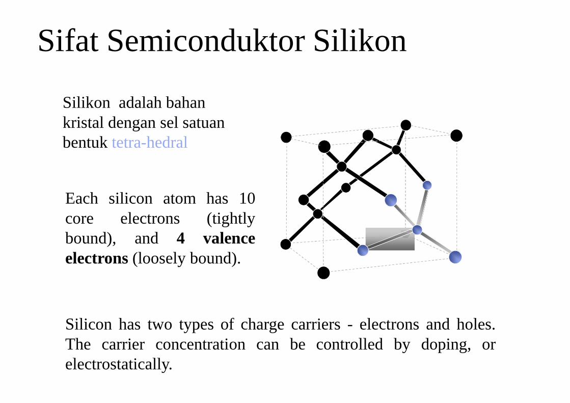
Silikon adalah bahan kristal dengan sel satuan bentuk tetra-hedral
Sifat Semiconduktor Silikon
Silicon has two types of charge carriers - electrons and holes.The carrier concentration can be controlled by doping, orelectrostatically.
Each silicon atom has 10core electrons (tightlybound), and 4 valenceelectrons (loosely bound).

Properties of Silicon Semiconductor(INTRISIC)
For simplicity we can consider a flattened model structure
At room temperature there are ~1 x 1010 cm-3 free carriers (electron or hole)
Holes and electrons canmove around the lattice, orrecombine to form acomplete bond.
Due to thermal effects somebonds are broken, givingmobile holes and electrons(charge carrier)
+ -

Example 2: Intrinsic Semiconductor at 300 K
- ---
+
+
+ +

Properties of Silicon Semiconductor(EXTRISIC)
Donor dopants increase the number of conduction electrons
P+
A donor atom, such asphosphorus, has fivevalence electrons, four ofwhich participate inbonding, leaving one extraelectron that is easilyreleased for conduction.The donor
site becomes positively charged (fixed charge).
Silicon doped with a donor is called n-type.

Properties of Silicon Semiconductor
Acceptor dopants increase the number of holes in the lattice
Silicon doped with an acceptor is called p-type.
An acceptor atom, such asboron, has three valenceelectrons, and cantherefore easily accept anelectron from a neighbour,leaving a free hole. Thedopant has a fixed negative
charge.
B-

Example 1: Doped Semiconductors
N-type P-type

Properties of Silicon Semiconductor
Overall doping depends on the relative number of acceptors anddonors.
Silicon doped with donorand acceptor atoms is calledCounter Doped, and canhave multiple separateregions of n- and p-typeconductivity
B- B-
P+

Properties of Silicon Semiconductor
The carriers distribution is also affected by electric fields
Between collisions withthe lattice the carriers areaccelerated in the directionof the electrostatic field.
B-
E
Combining the effects of doping and fields on the carrierconcentration and distribution, we can realise useful devices.

• Keboleh jadian suatu keadaan dengan energi E ditempati elektron dengan spin ½ yang memenuhi prinsip Pauli diberikan oleh fungsi sbb:
Fungsi distribusi dalam kesetimbangan
TkEE
Ef
B
Fn
exp1
1)(
• Fungsi distribusi Fermi-Diracberlaku dalam kesetimbangan termal.
• Untuk kondisi tak setimbang fungsi distribusi ini tidak berlaku.
fn(E)
1
1/2
T=0 K
T>0 K
EF=Tingkat Fermi (potensial elektrokima)

• Jika E-EF>>kBT, fungsi distribusi Fermi-Dirac distribution didekati menjadi fungsi distribusi Maxwell-Boltzmann :
• Kebolehjadian suatu keadaan tingkat energi tidak ditempati elektron adalah:
fp(E) menggambarkan kebolehjadian suatu tingkat energi ditempati hole.
TkEEEf
B
Fn exp)(
)(exp1
1
exp1
11)(1 Ef
TkEE
TkEE
Ef p
B
F
B
Fn

Perhitungan elektron(n) dan hole (p):• Konsentrasi elektron di dalam semikonduktor dihitung sbb:
• Jika diintroduksi variabel sbb:
• Maka diperoleh konsentrasi elektron (n):
dEEEm
dEEfEgn
TkEE
Ec
n
Enc
B
F
c
c
exp112
21
)()(
2/3
2
*
2
TkEE
TkEE
B
cF
B
c
,
2/3
2
*
2/12/122 ,)(
hTkmN
TkEEFNFNn Bn
cB
cFcc
Densitas efektif keadaanpada pita konduksi.

• Dengan cara yang sama konsentrasi hole sbb:
• Besarnya nilai Nc dan Nv untuk bebrapa semiconduktor pada T=300 K:
2/3
2
*
2/12/1
22 ,)(
hTkm
NTkEEFNFNp Bp
vB
Fvvv
Densitas Efektif keadaanpada pita valensi.
Material Nc [cm-3] Nv [cm-3]
Si 2.8x10¹⁹ 1.04x10¹⁹
Ge 1.04x10¹⁹ 6.0x10¹⁸
GaAs 4.7x10¹⁷ 7.0x10¹⁸

Integral Fermi-Dirac:• Definisi:
• Batasan kasus:
(a) <<1
(b) >>1
(c) -4<< <<4
02/1 exp1
2)( dF
eF )(2/1
3
4)(2/3
2/1F
)105117.110797.8045417.074041.032881.0exp()(
4434
22/1
F

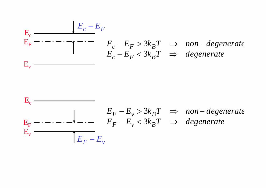
Semikonduktor degenerasi vs non-degenerasi • Jika EF berada diantara celah energi, dan berjarak dari tepi
pita konduksi atau pita valensi beberapa kali dari energi termal (kBT) semikonduktor (SC) disebut non-degenerasi
• Pada batas berlawanan, jika EF masuk ke pita konduksi atau pita valensi maka semikonduktor (SC) disebut degenerasi:
eF )(2/1
TkEE
Np
TkEE
Nn
B
Fvv
B
cFc
exp
exp
2/32/1 3
4)(
F
Ec
Ev
EF
Fc EE
degenerateTkEEdegeneratenonTkEE
BFcBFc
33
Ec
Ev
EF
vF EE
degenerateTkEEdegeneratenonTkEE
BvFBvF
33

Konsentrasi pembawa Intrinsik • Untuk SC non-degenerasi, kita dapatkan:
• Konsentrasi pembawa intrinsik untuk SC umum :
TkENNn
nTkENNpn
Bgvci
iBgvc
2exp
exp 2
Konsentrasi pembawa intrinsik => f(T,Eg)
Material Eg [eV] ni [cm-3]
Si 1.12 1.0x10¹⁰
Ge 0.66 2.4x10¹³
GaAs 1.424 1.79x10⁶

• Grafik ketergantungan temperatur konsentrasi pembawa intrisik sbb.
- T kamar => ni kecil dibanding tingkat doping- T tinggi => ni besar karena generasi termal pembawa
ln(ni)
1/T
Si GeGaAs
Slope ~ Eg

• Untuk semikonduktor SC intrinsik :n=ni and p=ni,
maka dapat ditentukan letak energi energi Fermi intrisik:
*
*
ln43
2 n
pB
vci m
mTkEEE
Tingkat energi Fermi intrinsik Ei SC terletak ditengah celah pita energi.
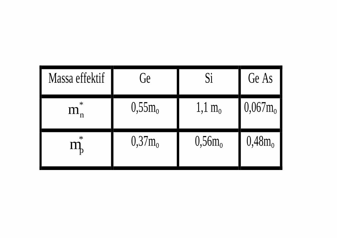
Massa effektif Ge Si Ge As
*nm
0,55mo 1,1 mo 0,067mo
*pm
0,37mo 0,56mo 0,48mo

• Klasifikasi semikonduktor: intrinsik (tanpa dopan, murni) extrinsik (adanya atom donor atau aseptor) compensated (baik impuritas donor and aseptor)
• Sifat donor and aseptor-sesuai dengan impuritas:Impuritas donor: pembawa muatan major e-
pembawa muatan minor e+
Impuritas aseptor: pembawa muatan major e+
pembawa muatan minor e-
Donor dan aseptor
Ec
Ev
Ed
Ec
Ev
Ea
T=0 K

• Perhitungan tingkat energi impuritas paling sederhana berdasarkan model atom hidrogen.
• Berdasarkan nilai Ec-Ed and Ea-Ev maka dapat dibedakan antara: - impuritas dangkal (shallow impurities)
- impuritas tingkat dalam (deep-level impurities)
• Banyaknya dopan terionisasi diformulasikan sbb:
eVqm
EH 2.1332 22
02
40
SieVEE
SieVEEmm
Eva
dc
n
Sid for 05.0
for 025.0/
/2.13 *0
20
TkEE
NN
TkEE
NN
B
dF
dd
B
Fa
aa
exp21,
exp41
=> Energi Ionisasi

Perhitungan tingkat Fermi • Tingkat Fermi mengatur dengan sendirinya untuk
menjamin netralitas muatan dalam semikonduktor. Kondisi netralitas muatan digabung dengan hukum aksi massa berlaku untuk SC degerasi dan non degernarsi, maka akan berlaku:
2i
dannp
NpNn=> Hukum aksi massa
2221
21
2221
21
4
4
idada
iadad
nNNNNp
nNNNNn
=> Netralitas muatan

• Contoh tipe-n (Na=0):
Limit T rendah:
22/122
41
])2
([2
1exp81ln
exp21)exp(
id
id
B
dc
c
dBdF
B
dF
dcd
nnpNnNn
TkEE
NNTkEE
TkEE
NNNn
c
dBdcTF N
NTkEEE2
ln22
0

Limit T tinggi:• Untuk SC tipe N
• Untuk SC tipe-P
• Variasi temperature dari EF:
a
vBvF N
NTkEE ln
d
cBcF N
NTkEE ln
Energi
Ec
Ev
Ei
Tipe-n
Tipe-p
T

• Ekspresi lain tingkat energi Fermi
)ln(
)exp()exp(
)exp()exp(
)exp()exp(
i
DiF
B
Fii
B
iFi
B
Fvv
B
ivvi
B
cFc
B
cici
nNkTEENtipeUntuk
TkEEnp
TkEEnn
TkEENp
TkEENn
TkEENn
TkEENn

• Variasi temperatur konsentrasi elektron n:
1/T
n/Nd
ni
1
ekstrinsikintrinsik
Freeze-out

Pita ImpuritasE
gc(E)
Ec
Ed
Doping rendah Nd
Ketika doping naik, fungsi gelombang donor menjadi tumpang tindih. Kita dapat menghi-tung ketebalan doping kritis menggunakan prinsip ketakpastian Heisenberg:
dengan:
Maka diperoleh
px
Tmkmvp Bthermal 3
318
23
23.
104
31
-
BcritD
cm
Tmkx
N

• Untuk memahami ini tinjau atom hidrogen
Egc(E)
Ec
Ed
Doping tinggi Nd
Tingkat donor diskrit melebar ke pita yang tumpang tindih dengan pita kondusi , menyebabkan celah energi menyempit=> band-gap narrowing effect
satu atom dua atomsKisi kristal
Tingkat Energi Anti-bonding
Bonding
C.B.
V.B.