konsep dasar sem
TRANSCRIPT
7/26/2019 Konsep Dasar SEM
http://slidepdf.com/reader/full/konsep-dasar-sem 1/29
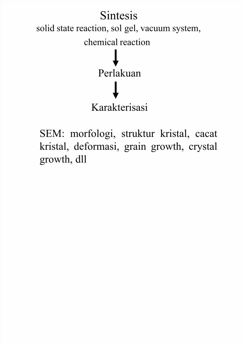
Sintesissolid state reaction, sol gel, vacuum system,
chemical reaction
Perlakuan
Karakterisasi
SEM: morfologi, struktur kristal, cacatkristal, deformasi, grain growth, crystalgrowth, dll

7/26/2019 Konsep Dasar SEM
http://slidepdf.com/reader/full/konsep-dasar-sem 2/29
Scanning Electron Microscope
7/26/2019 Konsep Dasar SEM
http://slidepdf.com/reader/full/konsep-dasar-sem 3/29
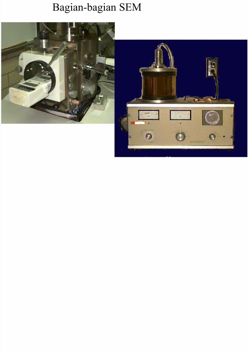
Bagian-agian SEM
7/26/2019 Konsep Dasar SEM
http://slidepdf.com/reader/full/konsep-dasar-sem 4/29
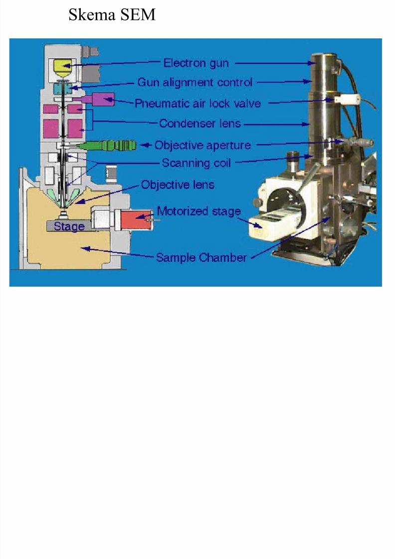
Skema SEM
7/26/2019 Konsep Dasar SEM
http://slidepdf.com/reader/full/konsep-dasar-sem 5/29
!eneral "ses:#Mengamati permukaan pada M$ %&-%&&&&& ',resolusi permukaan hingga kedalaman (-%&& nm
#)paila ditamahkan dengan detektorbackscattered , SEM erfungsi untuk:*%+mengamati grain oundaries pada sampel tanpa
etsa *+pengamatan daerah domain pada materialferromagnetic, *(+evaluasi orientasi kristalografigrain dengan diameter -%& µm, *.+pengamatanfasa lain akiat adanya peredaan rerata grain
7/26/2019 Konsep Dasar SEM
http://slidepdf.com/reader/full/konsep-dasar-sem 6/29
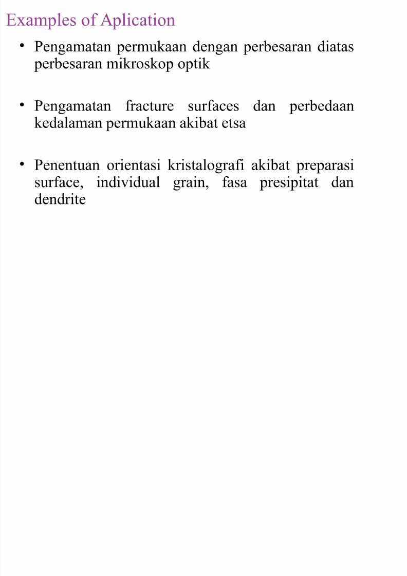
E/amples of )plication
# Pengamatan permukaan dengan peresaran diatas
peresaran mikroskop optik
# Pengamatan fracture surfaces dan peredaankedalaman permukaan akiat etsa
# Penentuan orientasi kristalografi akiat preparasisurface, individual grain, fasa presipitat dandendrite

7/26/2019 Konsep Dasar SEM
http://slidepdf.com/reader/full/konsep-dasar-sem 7/29
# 0dentifikasi elemen kimia dalam ukuran mikron pada ulk sample,eg inclusi, fasa presipitate
# Evaluasi gradien komposisi kimia pada
permukaan ulk sample
# Pengamatan pada semikonduktor devices untukfailure analysis, function control dan verifikasi
desain
E/amples of )plication
7/26/2019 Konsep Dasar SEM
http://slidepdf.com/reader/full/konsep-dasar-sem 8/29
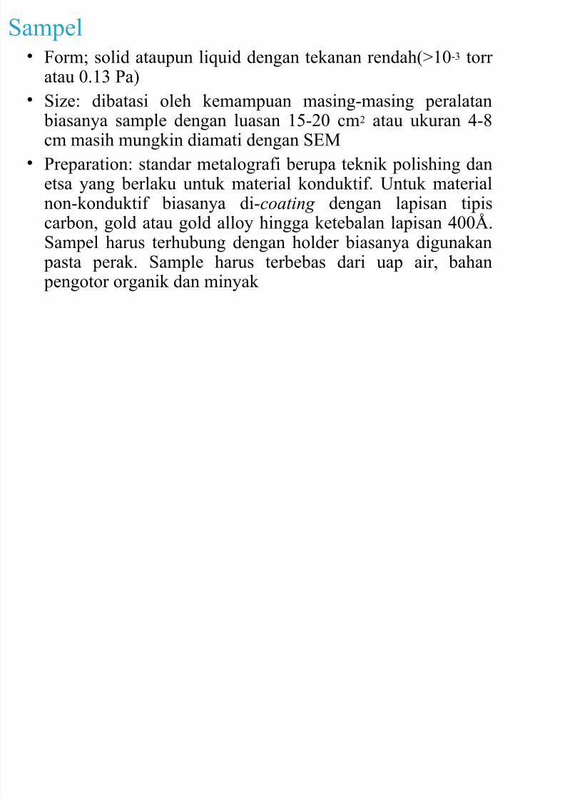
Sampel# 1orm solid ataupun li2uid dengan tekanan rendah*3%&-( torr
atau &4%( Pa+
# Si5e: diatasi oleh kemampuan masing-masing peralatan iasanya sample dengan luasan %6-& cm atau ukuran .-7cm masih mungkin diamati dengan SEM
# Preparation: standar metalografi erupa teknik polishing danetsa yang erlaku untuk material konduktif4 "ntuk materialnon-konduktif iasanya di-coating dengan lapisan tipiscaron, gold atau gold alloy hingga ketealan lapisan .&&84Sampel harus terhuung dengan holder iasanya digunakan pasta perak4 Sample harus tereas dari uap air, ahan pengotor organik dan minyak
7/26/2019 Konsep Dasar SEM
http://slidepdf.com/reader/full/konsep-dasar-sem 9/29
9apailities of related echni2ues
# '-ray ;iffraction: menyediakan informasikristalografi# Mikroskop <ptik: memerikan informasi
awal keadaan permukaan sampel
# ransmission electron microscopy:memerikan informasi keadaan materialsecara spesifik dislokasi, small angle
oundari distriution and vacancy cluster4

7/26/2019 Konsep Dasar SEM
http://slidepdf.com/reader/full/konsep-dasar-sem 10/29

7/26/2019 Konsep Dasar SEM
http://slidepdf.com/reader/full/konsep-dasar-sem 11/29
Kategori komponen dalam mikroskop elektron
%4 Electron column
4 Specimen chamer
(4 =acuum pumping system
.4 Electronic control and imaging system
7/26/2019 Konsep Dasar SEM
http://slidepdf.com/reader/full/konsep-dasar-sem 12/29
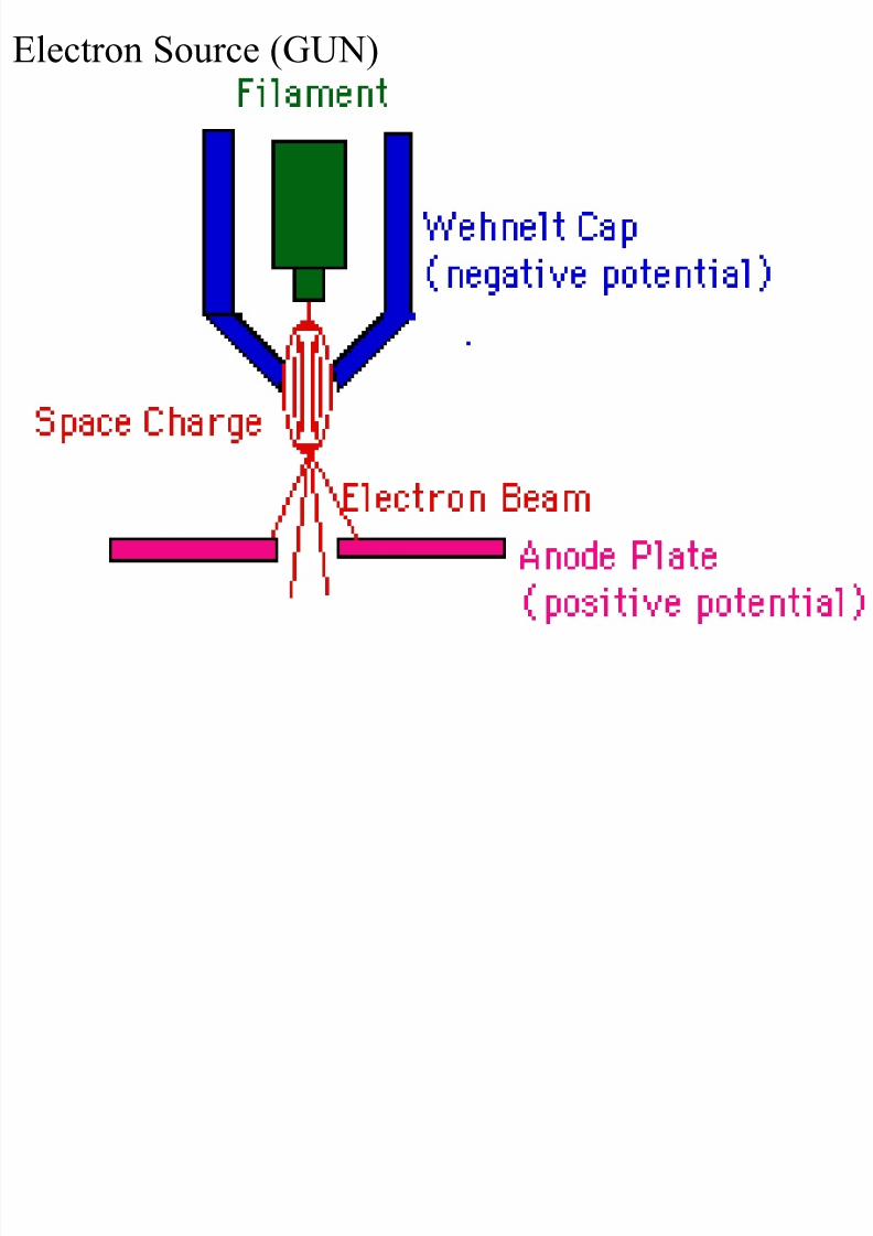
Electron Source *!">+

7/26/2019 Konsep Dasar SEM
http://slidepdf.com/reader/full/konsep-dasar-sem 13/29
) hermionic Electron !un functions in the following manner
%4 )n positive electrical potential is applied to the anode
4 he filament *cathode+ is heated until a stream of electrons is produced
(4 he electrons are then accelerated y the positive potential down the column
.4 ) negative electrical potential *?6&& =+ is applied to the @henelt 9ap
64 )s the electrons move toward the anode any ones emitted from the filamentAs side are repelled y the @henelt 9ap toward the optic a/is *hori5ontal center+
4 ) collection of electrons occurs in the space etween the filament tip and @henelt 9ap4 his collection is called a space charge
C4 hose electrons at the ottom of the space charge *nearest to the anode+ can e/it the gun area through the small *D% mm+ hole in the @henelt 9ap
74 hese electrons then move down the column to e later used in imaging
7/26/2019 Konsep Dasar SEM
http://slidepdf.com/reader/full/konsep-dasar-sem 14/29
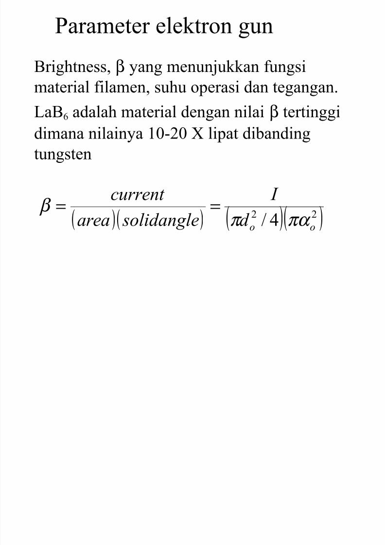
Parameter elektron gun
Brightness, β yang menunukkan fungsimaterial filamen, suhu operasi dan tegangan4
FaBB adalah material dengan nilai β tertinggi
dimana nilainya %&-& ' lipat diandingtungsten
( ) ( ) ( )( )--.G ood I
solidangleareacurrent
πα π β ==

7/26/2019 Konsep Dasar SEM
http://slidepdf.com/reader/full/konsep-dasar-sem 15/29
# he Broers design utili5es a tungstencoil wrapped around the pointed endof a long *around cm+ FaB rod4his design uses the heat radiationand electron omardment from the
tungsten coil to heat the very end ofthe tip4 he conduction of heatthrough the cathode holder, locatedat the other end of the rod, helps tolessen the prolems of the reactivityof the material4
# =ogel proposed a short FaB rodheated directly y passing a currentthrough the FaB rod, perpendicularto the length of the rod4 his isaccomplished y using rigidelectrical connectors that also
provide the support for the rod4# 0n the design of 1erris et al.C, a short
FaB rod is supported y a rion orstrip through which an electricalcurrent is passed for heating4 he rod
is heated y conduction from therion4

7/26/2019 Konsep Dasar SEM
http://slidepdf.com/reader/full/konsep-dasar-sem 16/29
Specimen 0nteraction
7/26/2019 Konsep Dasar SEM
http://slidepdf.com/reader/full/konsep-dasar-sem 17/29
Backscattered Electrons:
Formation
9aused y an incident electron colliding with an atom in the specimen which isnearly normal to the incidentAs path4 he incident electron is then scatteredHackwardH %7& degrees4
Utilization he production of ackscattered electrons varies directly with the specimenAs atomicnumer4 his differing production rates causes higher atomic numer elements toappear righter than lower atomic numer elements4 his interaction is utili5ed todifferentiate parts of the specimen that have different average atomic numer4 )ne/ample is shown in the SEM output section, specifically the mechanically alloyedspecimen micrograph
7/26/2019 Konsep Dasar SEM
http://slidepdf.com/reader/full/konsep-dasar-sem 18/29
Secondary Electrons:
Source
9aused y an incident electron passing HnearH an atom in the specimen, nearenough to impart some of its energy to a lower energy electron *usually in the K-shell+4 his causes a slight energy loss and path change in the incident electron andthe ioni5ation of the electron in the specimen atom4 his ioni5ed electron thenleaves the atom with a very small kinetic energy *6e=+ and is then termed aHsecondary electronH4 Each incident electron can produce several secondaryelectrons4Utilization
Production of secondary electrons is very topography related4 ;ue to their lowenergy, 6e=, only secondaries that are very near the surface *D%&nm+ can e/it thesample and e e/amined4 )ny changes in topography in the sample that are larger
than this sampling depth will change the yield of secondaries due to collectionefficiencies4 9ollection of these electrons is aided y using a HcollectorH inconunction with the secondary electron detector4 he collector is a grid or meshwith a I%&&= potential applied to it which is placed in front of the detector,attracting the negatively charged secondary electrons to it which then pass through
the grid-holes and into the detector to e counted4
7/26/2019 Konsep Dasar SEM
http://slidepdf.com/reader/full/konsep-dasar-sem 19/29
Auger Electrons
Source
9aused y the de-energi5ation of the specimen atom after a secondary electron is produced4 Since a lower *usually K-shell+ electron was emitted from the atomduring the secondary electron process an inner *lower energy+ shell now has avacancy4 ) higher energy electron from the same atom can HfallH to a lowerenergy, filling the vacancy4 his creates and energy surplus in the atom which can
e corrected y emitting an outer *lower energy+ electron an )uger Electron4Utilization
)uger Electrons have a characteristic energy, uni2ue to each element from whichit was emitted from4 hese electrons are collected and sorted according to energyto give compositional information aout the specimen4 Since )uger Electrons
have relatively low energy they are only emitted from the ulk specimen from adepth of D(

7/26/2019 Konsep Dasar SEM
http://slidepdf.com/reader/full/konsep-dasar-sem 20/29
X-rays
Source
9aused y the de-energi5ation of the specimen atom after a secondary electron is produced4 Since a lower *usually K-shell+ electron was emitted from the atomduring the secondary electron process an inner *lower energy+ shell now has avacancy4 ) higher energy electron can HfallH into the lower energy shell, filling thevacancy4 )s the electron HfallsH it emits energy, usually '-rays to alance the total
energy of the atom so it 4Utilization
'-rays or Fight emitted from the atom will have a characteristic energy which isuni2ue to the element from which it originated4 hese signals are collected andsorted according to energy to yield micrometer diameter+ of ulk specimens
limiting the point-to-point comparisons availale
7/26/2019 Konsep Dasar SEM
http://slidepdf.com/reader/full/konsep-dasar-sem 21/29
Thin Specimen Interactions
"nscattered Electrons
Source 0ncident electrons which are transmitted through the thin specimen without anyinteraction occurring inside the specimen4
Utilization he transmission of unscattered electrons is inversely proportional to thespecimen thickness4 )reas of the specimen that are thicker will have fewertransmitted unscattered electrons and so will appear darker, conversely thethinner areas will have more transmitted and thus will appear lighter4

7/26/2019 Konsep Dasar SEM
http://slidepdf.com/reader/full/konsep-dasar-sem 22/29
Elasticity Scattered electrons
Source
0ncident electrons that are scattered *deflected from their original path+ y atoms inthe specimen in an elastic fashion *no loss of energy+4 hese scattered electrons arethen transmitted through the remaining portions of the specimen4
Utilization
)ll electrons follow BraggAs Faw and thus are scattered according to@avelength$JSpace etween the atoms in the specimenJsin*angle of scattering+4)ll incident electrons have the same energy*thus wavelength+ and enter thespecimen normal to its surface4 )ll incidents that are scattered y the same atomicspacing will e scattered y the same angle4 hese Hsimilar angleH scatteredelectrons can e collated using magnetic lenses to form a pattern of spots each spot
corresponding to a specific atomic spacing *a plane+4 his pattern can then yieldinformation aout the orientation, atomic arrangements and phases present in thearea eing e/amined4
7/26/2019 Konsep Dasar SEM
http://slidepdf.com/reader/full/konsep-dasar-sem 23/29
Inelastically Scattered Electrons
Source
0ncident electrons that interact with specimen atoms in a inelastic fashion, loosingenergy during the interaction4 hese electrons are then transmitted trough the rest ofthe specimen
Utilization 0nelasticaly scattered electrons can e utili5ed two ways
#Electron Energy Foss Spectroscopy: he inelastic loss of energy y theincident electrons is characteristic of the elements that were interacted with4hese energies are uni2ue to each onding state of each element and thus can eused to e/tract oth compositional and onding *i4e4 o/idation state+information on the specimen region eing e/amined4
#Kakuchi Bands: Bands of alternating light and dark lines that are formed yinelastic scattering interactions that are related to atomic spacings in thespecimen4 hese ands can e either measured *their width is inversely proportional to atomic spacing+ or HfollowedH like a roadmap to the HrealHelasticity scattered electron pattern4

7/26/2019 Konsep Dasar SEM
http://slidepdf.com/reader/full/konsep-dasar-sem 24/29
7/26/2019 Konsep Dasar SEM
http://slidepdf.com/reader/full/konsep-dasar-sem 25/29
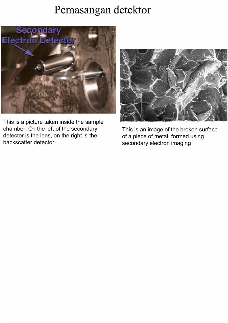
Pemasangan detektor
This is an image of the broken surface
of a piece of metal, formed using
secondary electron imaging
This is a picture taken inside the samplechamber. On the left of the secondary
detector is the lens, on the right is the
backscatter detector.
7/26/2019 Konsep Dasar SEM
http://slidepdf.com/reader/full/konsep-dasar-sem 26/29
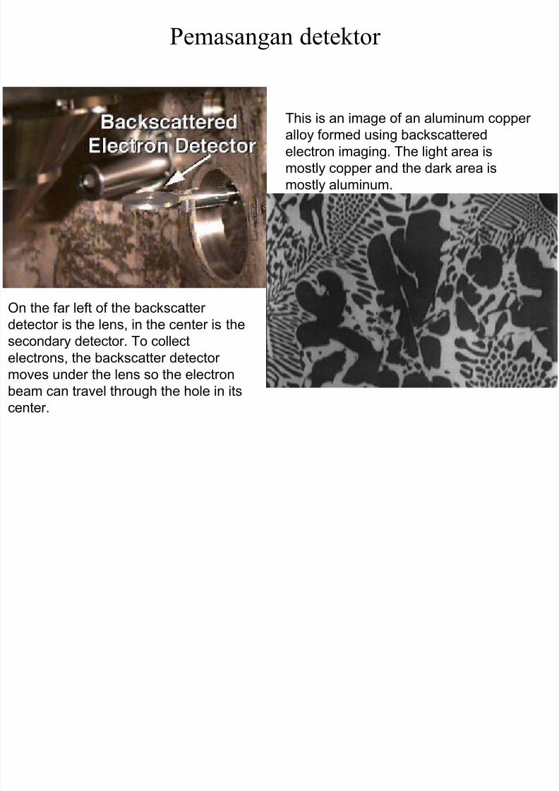
Pemasangan detektor
On the far left of the backscatter
detector is the lens, in the center is the
secondary detector. To collect
electrons, the backscatter detector
moves under the lens so the electron
beam can travel through the hole in itscenter.
This is an image of an aluminum copper
alloy formed using backscattered
electron imaging. The light area is
mostly copper and the dark area is
mostly aluminum.
7/26/2019 Konsep Dasar SEM
http://slidepdf.com/reader/full/konsep-dasar-sem 27/29
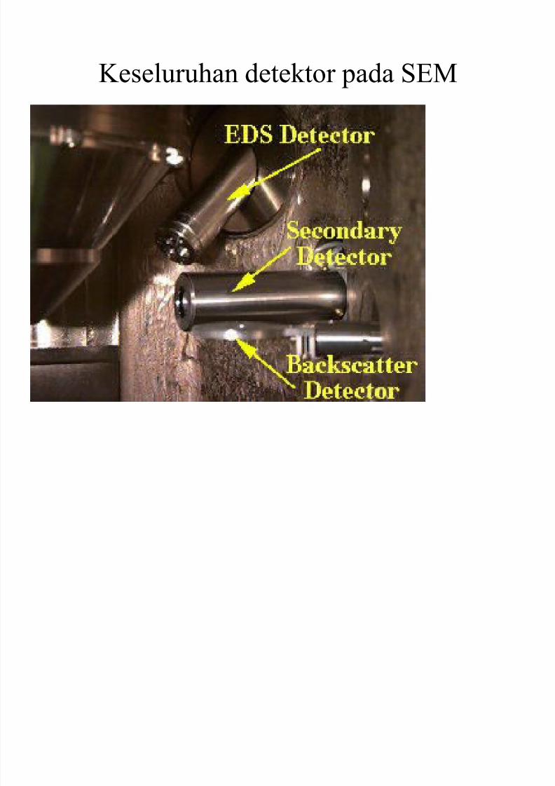
Keseluruhan detektor pada SEM
7/26/2019 Konsep Dasar SEM
http://slidepdf.com/reader/full/konsep-dasar-sem 28/29
Sistem ;etektor # ;etektor Secondary Electron *SE+ untuk menghasilkan
gamar analisis struktur mikro, analisis produk korosi,
patahan, kegagalan material# ;etektor Backscattered Electron *BSE+ untuk menghasilkan
gamar topografi peta struktur mikro yang gamarnyadientuk dari peredaan nomor atomGdensitas yang dikandungoleh ahan4 ;aerah cuplikan dengan nomer atom yang leihtinggi akan terlihat relatif leih terang daripada daerah dengannomer atom rendah
# ;etektor sinar-/ *SiFi+ dan E;'GE;S untuk analisiskomposisi unsur yang terkandung dalam orde micrometer dan
pemetaan *distriusi unsur+ dalam suatu ahan
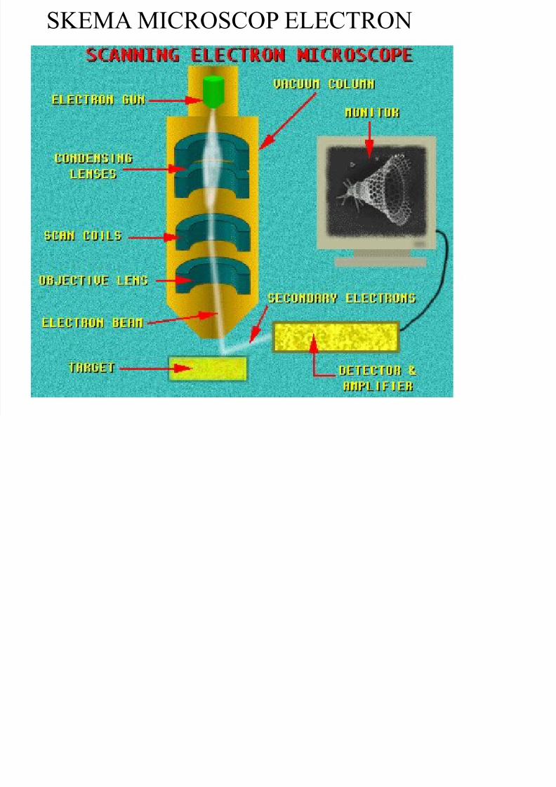
SKEM) M09<S9<P EFE9<>
7/26/2019 Konsep Dasar SEM
http://slidepdf.com/reader/full/konsep-dasar-sem 29/29
SKEM) M09<S9<P EFE9<>