electrical conductivity and surface roughness...
TRANSCRIPT
Electrical Conductivity and Surface Roughness Properties of Ferroelectric Gallium Doped Ba0,5Sr0,5TiO3 (BGST) Thin Films R.A. Hamdani1) (a), M. Komaro (a), Irzaman(b) (a) Department of Mechanical Engineering of Education FPTK UPI, Jl. Setiabudhi no.207 Bandung Indonesia – 40154 (b) Departement of Physic IPB, Jl.Raya Dramaga Bogor Indonesia. PACS : 72.80.-r; 73.61.-r; 74.62.Bf; 74.62.Dh; 77.70.+a; 77.84.Dy; 79.20.-m.
Abstract
Ba0.5Sr0.5TiO3 (BST) and gallium doped BST (BGST) thin films were
successfully deposited on p-type Si(100) substrates. The thin films were fabricated by the
chemical solution deposition (CSD) and spin coating method, with 1.00 M precursor and
spinning speed of 3000 rpm for 30 seconds. The post deposition annealing of the 9 films
were carried out BST without gallium (BGST 0%) annealing 850OC, BGST 0%
annealing 900OC, BGST 0% annealing 950OC, BGST 5% annealing 850OC, BGST 5%
annealing 900OC, BGST 5% annealing 950OC, BGST 10% annealing 850OC, BGST 10%
annealing 900OC, BGST 10% annealing 950OC for 15 hour in oxygen gas atmosphere,
respectively. The resistance and electrical conductivity of the grown thin films are
characterized by I-V converter, meanwhile surface roughness of the grown thin films are
characterized by atomic force microscopy (AFM) method. The electrical conductivity of
the grown thin films BGST due to semiconductor. The results show that resistance and
electrical conductivity of the thin film have strong correlation to the annealing
temperature, concentration dopant and surface roughness.
Keywords : Electrical conductivity, surface roughness, BST, dopant gallium, AFM.
________________________________ 1) Corresponding author; Phone/fax : +62 22 2020162, e-mail: [email protected], [email protected]
1. Introduction
Ferroelectric BaTiO3 (BT), Ba0.5Sr0.5TiO3 (BST), PbZr0.5Ti0.5O3 (PZT) thin
films are well known as dielectric materials. They have been used as capacitors and
high density dynamic random access memory (DRAM) due to their high dielectric
constant and high capacity of charge storage [1-4] and ferroelectric solar cell [5]. BT
and BST films can be formed by various methods, such as CSD [1-4], metal organic
chemical vapor deposition (MOCVD) [6,7], rf sputtering [3, 8, 10] and Pulsed Laser
Ablation Deposition (PLAD) [11]. CSD method is of particular interest because of its
good control of stoichiometry, ease of fabrication and low temperature synthesis. Since
it is relatively new, hence a greater understanding is required before the film quality
can be optimized. It was reported that CSD derived thin films are thermodinamically
stable [4].
Gallium oxide doped barium strontium titanate has been of immense interest in
the use of ferroelectric solar cell (FSC) [5]. The electrical conductivity properties of the
materials can be tailored by varying the concentration of the dopant and annealing
temperature. Since the sensors performance significantly depend on these properties,
the FSC performance can then be optimized.
In this paper we report on the fabrication of 0 % 5 %, 10 % gallium oxide doped
barium strontium titanate thin films by CSD with 1.00 M precursor. The electrical
conductivity properties using I-V converter characterization, meanwhile surface
roughness of the grown thin films are characterized by atomic force microscopy (AFM)
method. The electrical conductivity properties of the grown films related to the dopant
gallium oxide, annealing temperature and surface roughness are described.
2. Methodology
BGST 5 % solution was obtained using 0.160 g barium acetic [Ba(CH3COO)2,
99 % purity] + 0.131 g strontium acetic [Sr(CH3COO)2, 99 % purity] + 0.355 g
titanium isopropoxide [Ti(C12O4H28), 99.999 % purity] + 0.030 g gallium oxide as
precursor in 1.25 ml 2-methoxyethanol [H3COOCH2CH2OH, 99.9 %]. While BGST
10 % solution was obtained using 0.160 g barium acetic [Ba(CH3COO)2, 99 % purity]
+ 0.131 g strontium acetic [Sr(CH3COO)2, 99 % purity] + 0.355 g titanium
isopropoxide [Ti(C12O4H28), 99.999 % purity] + 0.060 g gallium oxide as precursor in
1.25 ml 2-methoxyethanol [H3COOCH2CH2OH, 99.9 %]. After 2 hours of agitating,
a thicken solution with a milky appearance was produced. After a filtering process a
clear solution was obtained. The solutions obtained, contain 1.00 M BGST 0 %, 5 %,
10%, respectively. The solutions were then spin coated on 10 mm x 10 mm p-type Si
(100) substrates with speed of 3000 rpm for 30 seconds . The post deposition
annealing of the films were carried out in a Nabertherm Type 27 model furnace at
850oC, 900oC, 950oC for 15 hours in an oxygen atmosphere [12,13]. The electrical
conductivity of the grown thin films were characterized by I-V converter, and surface
roughness of the grown thin films are characterized by atomic force microscopy (AFM)
method Model JEOL SPA300/400.
3. Results and Discussion
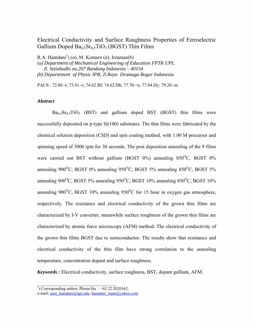
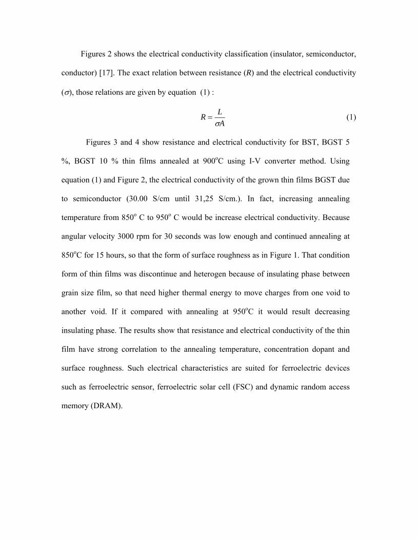
Figures 1 shows 3-dimensional images using AFM method of the thin films
annealed at temperatures 900oC. The surface roughness and grain size for BGST 5
% thin film annealed at 900oC were more homogenous, compared to BST and BGST
10 % thin films. The rms surface roughness for BST, BGST 5 %, BGST 10 % are
1.813 nm, 1.773 nm, 6.991 nm, respectively, whereas the grain size (mean diameter)
are 276.8 nm, 250.8 nm, 250.8 nm. Observation indicates a homogenous surface
obtained for BGST 5 % at 900oC. It can be seen that the introduction of Ga into BST
resulted in the improvement of the surface roughness and mean diameter grain size
(smaller surface roughness and mean diameter grain size). Many applications of the
surface roughness and mean diameter grain size of nanofabrication techniques now
require the production of nanowires. The nanowires could be used in a near feature as
components of technology to create electrical circuits out of compounds that are
capable of being formed into extremely small circuit (electronic, opto-electronic and
nanoelectromechanical devices and as leads for biomolecular nanosensors). Instead of
tunneling current, AFM techniques are capable to detect the interatomic forces that
occur between a cantilever probe tip and a sample. Normal imaging forces are in the 1 -
50 nanonewton range and cantilever deflections of less than 0.1 nm can be detected
(nanoscale) [14,15,16].
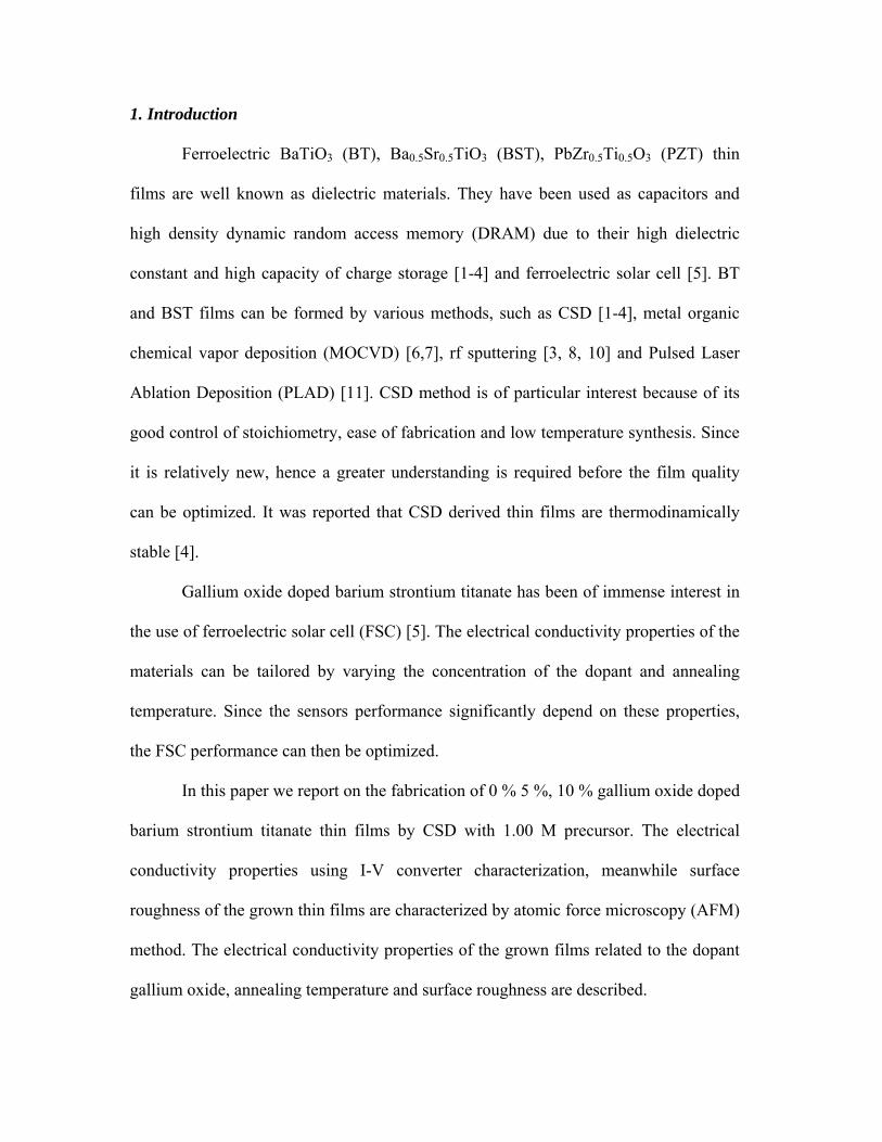
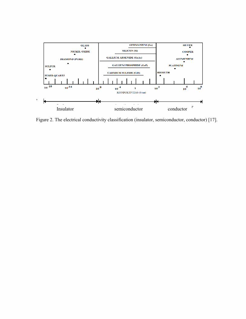
Figures 2 shows the electrical conductivity classification (insulator, semiconductor,
conductor) [17]. The exact relation between resistance (R) and the electrical conductivity
(σ), those relations are given by equation (1) :
ALRσ
= (1)
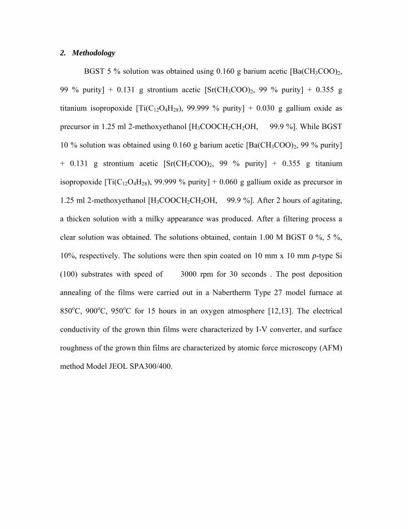
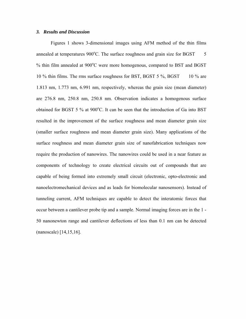
Figures 3 and 4 show resistance and electrical conductivity for BST, BGST 5
%, BGST 10 % thin films annealed at 900oC using I-V converter method. Using
equation (1) and Figure 2, the electrical conductivity of the grown thin films BGST due
to semiconductor (30.00 S/cm until 31,25 S/cm.). In fact, increasing annealing
temperature from 850o C to 950o C would be increase electrical conductivity. Because
angular velocity 3000 rpm for 30 seconds was low enough and continued annealing at
850oC for 15 hours, so that the form of surface roughness as in Figure 1. That condition
form of thin films was discontinue and heterogen because of insulating phase between
grain size film, so that need higher thermal energy to move charges from one void to
another void. If it compared with annealing at 950oC it would result decreasing
insulating phase. The results show that resistance and electrical conductivity of the thin
film have strong correlation to the annealing temperature, concentration dopant and
surface roughness. Such electrical characteristics are suited for ferroelectric devices
such as ferroelectric sensor, ferroelectric solar cell (FSC) and dynamic random access
memory (DRAM).
4. Conclusions
Fabrication of BST, BGST 5 %, BGST 10 % thin films were carried out by spin
coating at 3000 rpm for 30 seconds, and then annealing at 850oC, 900oC, 950oC, for
15 hours. The results show that resistance and electrical conductivity of the thin film
have strong correlation to the annealing temperature, concentration dopant and surface
roughness. with optimum structure obtained at 900oC.
Acknowledgment
This work was supported by Hibah Pekerti Project 2006 DP2M DIKTI, The
Republic of Indonesia.
References [1] J. Y. Seo, S. W. Park. Journal of Korean Physical Society, Vol 45, No.3, 769-
772 (2004). [2] Y.T. Raksa, M. Hikam, Irzaman. Ceramics International, 30, 1483 – 1485 (2004). [3] Irzaman, Y. Darvina, A. Fuad, P. Arifin, M. Budiman and M. Barmawi. phys.
stat. sol. (a) 199, No.3, 416-424 (2003). [4]. B.A. Baumert, L.H. Chang, A.T. Matsuda and C.J. Tracy. J. Mater. Res. 13, No.
1, 197 –204 (1998). [5] R.W. Miles. Science Direct, Vacuum, 80, 1090-1097 (2006). [6] B. Galiana, I. R. Stole, M.Baudrit, I. Garcia and C. Algora. Institute of physics
publishing, Semicond, Sci. Technol, 21, 1387-1392 (2006). [7] Y. Gao, and S. He. J. Appl. Phys., 87, No. 1, 124 – 132 (2000). [8]. T. Kawakubo, K. Abe, S. Komatsu, K. Sano, N. Yanase and H. Mochizuki.
IEEE Electron Device Letters. 18, No. 11, 529 – 531 (1997). [9]. J.S. Lee, J.S. Park, J.S. Kim, J.H. Lee, Y.H. Lee and S.R. Hanhn. J. Appl. Phys.,
38, No. 5B, page L574 – L576 (1999). [10] J. Miao, Y. Wang, H. Y. Tian, X. Y. Zhou, H. L. W. Chan, C.L. Choy, L. X.
Cao and B.R.Zhao. J. Phys. D: Appl. Phys., 39, 2565-2570 (2006). [11]. S. Kim, T.S. Kang and J.H. Je. J. Mater. Res., 14, No. 7, 2905 – 2911 (1999). [12] R.A. Hamdani, M. Komaro, Irzaman, A.C.W. Utami, A. Maddu. Jurnal Agritek
IPM Malang, 15, No. 4, 896 – 904 (2007).
[13] M. Komaro, R.A. Hamdani, Irzaman, A. Marwan, A. Arif. Jurnal Agritek IPM Malang, 15, No. 4, 970 – 973 (2007).
[14]. B.A. Long, S.H.U. Jian, S.U.N. Ping, L.U. Zu-Hong. Chin. Phys. Lett., 20, No. 4, 465 (2003)
[15]. I. Ratera, J. Chen1, A Murphy, D.F. Ogletree1, J.M.J. Fr´echet and M. Salmeron. Nanotechnology, 16, S235 (2005).
[16]. D Dietzel, Marc Faucher, Antonio Iaia, J PAim´e, S Marsaudon, A.M. Bonnot, V Bouchiat and G Couturier. Nanotechnology, 16, S73 (2005).
[17] K.N. Kwok. Complete Guide To Semiconductor Device, McGraw-Hill, inc., (1995).
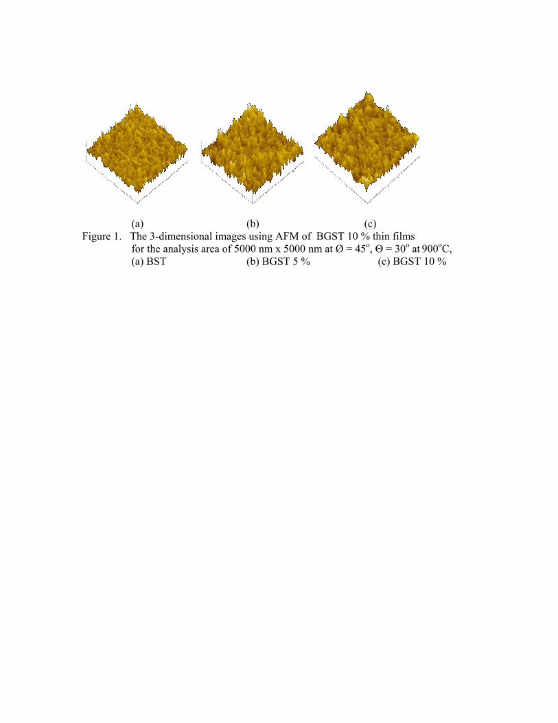
(a) (b) (c) Figure 1. The 3-dimensional images using AFM of BGST 10 % thin films
for the analysis area of 5000 nm x 5000 nm at Ø = 45o, Θ = 30o at 900oC, (a) BST (b) BGST 5 % (c) BGST 10 %
,
Insulator semiconductor conductor
Figure 2. The electrical conductivity classification (insulator, semiconductor, conductor) [17].
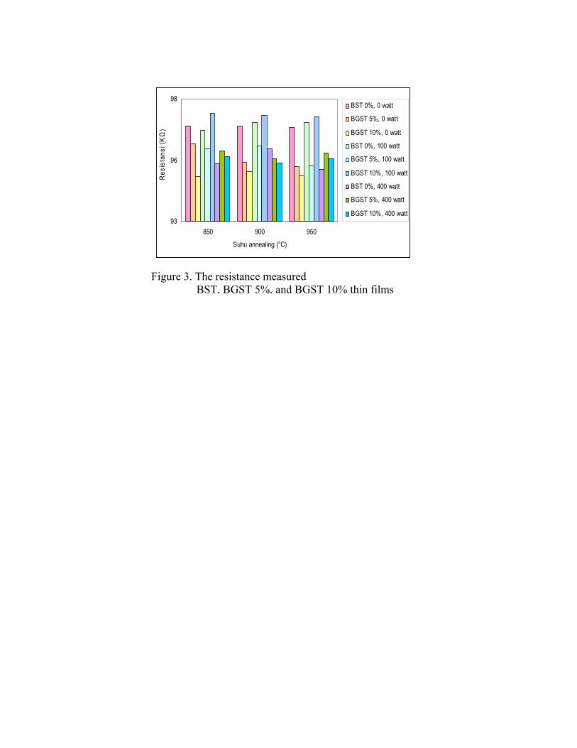
Figure 3. The resistance measured BST, BGST 5%, and BGST 10% thin films
93
96
98
850 900 950
Suhu annealing (°C)
Res
ista
nsi (
KΩ
)
BST 0%, 0 watt
BGST 5%, 0 watt
BGST 10%, 0 watt
BST 0%, 100 watt
BGST 5%, 100 watt
BGST 10%, 100 watt
BST 0%, 400 watt
BGST 5%, 400 watt
BGST 10%, 400 watt
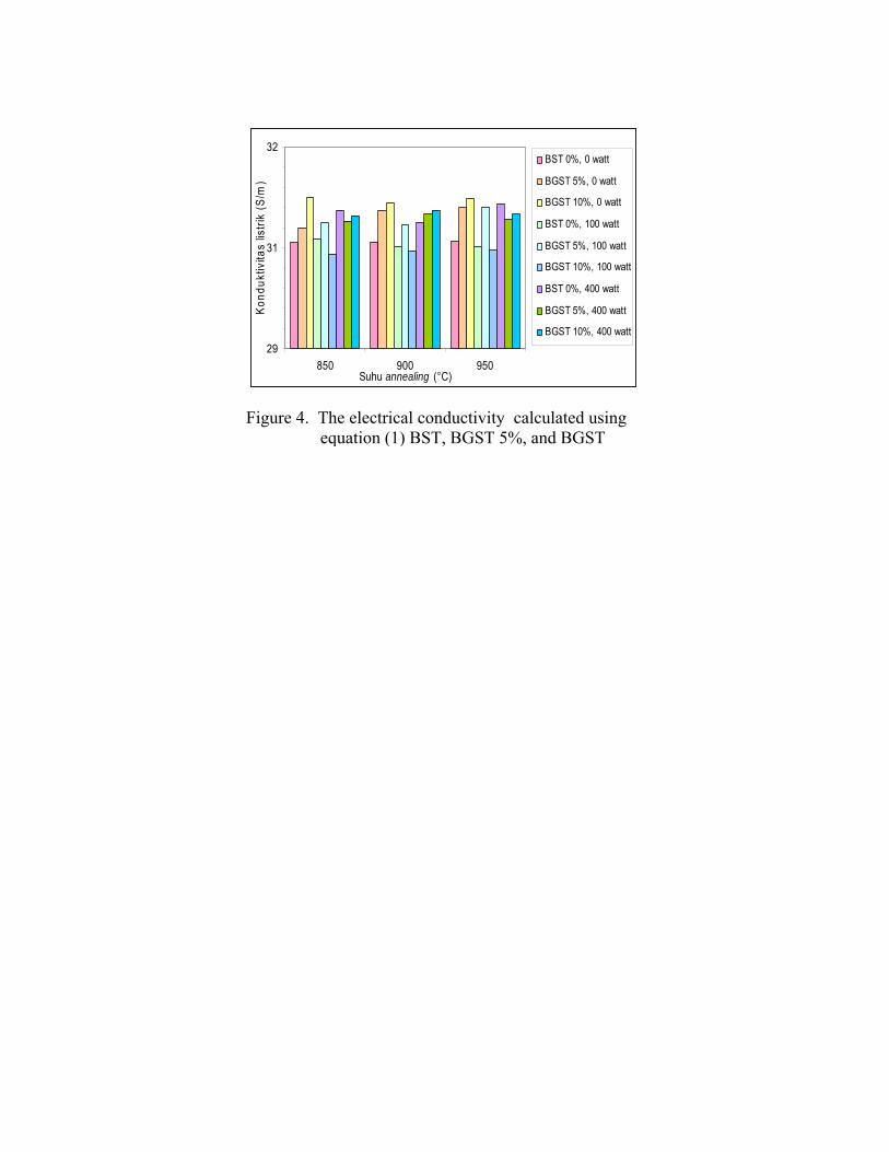
Figure 4. The electrical conductivity calculated using equation (1) BST, BGST 5%, and BGST
29
31
32
850 900 950Suhu annealing (°C)
Kond
uktiv
itas
listri
k (S
/m)
BST 0%, 0 watt
BGST 5%, 0 watt
BGST 10%, 0 watt
BST 0%, 100 watt
BGST 5%, 100 watt
BGST 10%, 100 watt
BST 0%, 400 watt
BGST 5%, 400 watt
BGST 10%, 400 watt
