© 2008 WILEY-VCH Verlag GmbH & Co. KGaA, Weinheim
p s scurrent topics in solid state physics
c
statu
s
soli
di
www.pss-c.comph
ysi
caphys. stat. sol. (c) 5, No. 6, 2108–2110 (2008) / DOI 10.1002/pssc.200778460
InGaN/GaN laser diodes on semipolar (1011) bulk GaN substrates
Anurag Tyagi*,1, Hong Zhong1, Roy B. Chung1, Daniel F. Feezell1, Makoto Saito1, Kenji Fujito2, James S. Speck1, Steven P. DenBaars1, and Shuji Nakamura1
1 Materials Department and Electrical and Computer Engineering Department, University of California,
Santa Barbara, CA 93106, USA 2 Optoelectronics Laboratory, Mitsubishi Chemical Corporation, 1000 Higashi-Mamiana, Ushiku, Ibaraki 300-1295, Japan
Received 5 September 2007, accepted 12 January 2008
Published online 27 March 2008
PACS 42.55.Px, 78.47.+p, 78.55.Cr, 78.60.Fi, 78.67.De
* Corresponding author: e-mail [email protected], Phone: +01 805 893 8869, Fax: +01 805 893 8983
© 2008 WILEY-VCH Verlag GmbH & Co. KGaA, Weinheim
1 Introduction Current commercial nitride based de-vices, grown along the polar [0001] c-direction, are charac-terized by the presence of polarization-induced electric fields in the biaxially compressively strained InGaN multi-quantum wells (MQWs) [1]. These electric fields, caused by both discontinuities in spontaneous and piezoelectric polarization at heterointerfaces, lead to the quantum con-fined Stark effect (QCSE) and reduced radiative recombi-nation probability [2, 3]. To circumvent these detrimental effects on device performance, it is desirable to grow In-GaN/GaN heterostructures with reduced or non-existent in-ternal piezoelectric fields. To this end, growth of nitride based optoelectronic devices on crystal planes other than the commonly used c-plane, e.g. nonpolar {10-10} (m-plane) and {11-20} (a-plane), and semipolar {10-1-1}, {10-1-3}, {11-22} planes, has been proposed [4-11]. Fur-thermore, higher optical gain and lower effective hole masses are theoretically anticipated from these quantum well (QW) structures with unequal biaxial in-plane stress [12-14]. Recently, the first nonpolar InGaN/GaN laser diodes (LDs) have been demonstrated [15-18]. In this talk we present the first results on semipolar (10-1-1) InGaN/GaN LDs [19].
2 Experimental 2.1 Growth The LD structure was grown by conven-tional metal organic chemical vapor deposition (MOCVD) on hydride vapor phase epitaxy (HVPE) grown low ex-tended defect density semipolar (10-1-1) bulk GaN sub-strates (provided by Mitsubishi Chemical Corp.). The LD structures were grown at atmospheric pressure (AP), with typical V/III ratios (>3000), and using typical temperature ranges (850 to 1200 ˚C). A GaN:Si layer was grown on top of the substrate, followed by a 30 nm InGaN compliance layer and a 250 period 1.5/1.5 nm AlGaN/GaN Si-doped n-cladding layer. Next, a 100 nm GaN:Si separate confine-ment heterostructure (SCH) was grown followed by a 5-period InGaN/GaN (5/8 nm) undoped MQW active region. The active region was then capped with a 10 nm p-doped AlGaN electron blocking layer. A 60-nm-thick p-GaN SCH was then grown, followed by a 125 period 1.5/1.5 nm AlGaN/GaN Mg-doped p-cladding layer. Finally, a 150 nm p-type GaN layer with a 20 nm p++ GaN contact layer was grown. 2.2 Fabrication The fabrication of the gain guided broad area laser diodes consisted of lithographically pat-
The first semipolar nitride laser diodes (LDs) have been real-
ized on low extended defect density semipolar ( )1011 GaN
bulk substrates. The LDs were grown by conventional metal
organic chemical vapor deposition (MOCVD). Broad area la-
sers with uncoated etched facets were fabricated and tested
under pulsed conditions. Lasing was observed at a duty cycle
of 0.025% with the threshold current density (Jth) being 24.5
kA/cm2 for a 5 µm × 800 µm device. An output power of 65
mW was measured from a single facet of the device at a drive
current of 1.5 A, with the calculated differential quantum ef-
ficiency (ηdiff) being 8%. Stimulated emission was observed at
405.9 nm with a narrow full width half maximum (FWHM)
of less than 0.3 nm. The lowest measured Jth was 16.5
kA/cm2 for a 10 µm × 800 µm device.
phys. stat. sol. (c) 5, No. 6 (2008) 2109
www.pss-c.com © 2008 WILEY-VCH Verlag GmbH & Co. KGaA, Weinheim
Contributed
Article
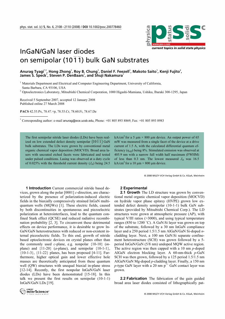
terning a thin metal stripe (Pd/Au) for current injection, mesa and laser facet formation via reactive ion etching (RIE), and evaporation of n-metal contacts (Ti/Al/Au) and p-metal pads. The laser stripes were oriented parallel to the projection of the c-axis on the epitaxial surface i.e. [10-1-2]. 2.3 Testing The testing was performed under pulsed conditions on laser bars without any heat sinking. All data was collected under a 200 µs period and 50 ns pulse width, corresponding to a 0.025% duty cycle. The stimulated emission spectrum was collected by coupling the output light from a single facet into a multi-mode fiber routed into an optical spectrum analyzer (OSA) with a resolution of 0.05 nm. 3 Results and discussion Figure 1 shows light vs. current (L-I) curve for the laser diode with a cavity length of 800 µm and a stripe width of 5 µm. Clearly defined threshold characteristics were observed in the L-I curve, with the threshold current (Ith) being ~1 A. The corre-sponding threshold current density (Jth) and threshold volt-age (Vth) were 24.5 kA/cm2 and ~12 V, respectively. An output power of 65 mW, at a pulsed current of 1.5 A, was measured from a single (uncoated) facet of the semipolar laser diode. The calculated differential quantum efficiency (ηdiff) was 8%.The relatively high threshold current density and voltage are attributable to unoptimized epitaxial growth and device fabrication.
Figure 1 Pulsed L-I characteristics using 50 ns pulses at a 5 kHz
repetition rate for broad area semipolar ( )1110 laser diode.
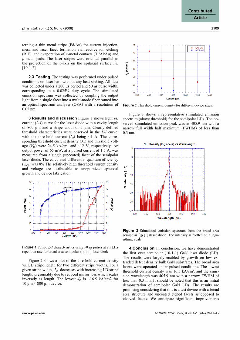
Figure 2 shows a plot of the threshold current density vs. LD stripe length for two different stripe widths. For a given stripe width, Jth decreases with increasing LD stripe length, presumably due to reduced mirror loss which scales inversely as length. The lowest Jth is ~16.5 kA/cm2 for 10 µm × 800 µm device.
Figure 2 Threshold current density for different device sizes.
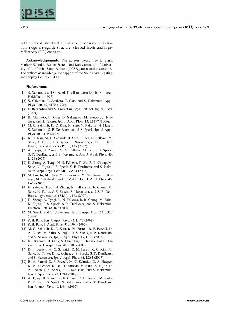
Figure 3 shows a representative stimulated emission spectrum (above threshold) for the semipolar LDs. The ob-served stimulated emission peak was at 405.9 nm with a narrow full width half maximum (FWHM) of less than 0.3 nm.
Figure 3 Stimulated emission spectrum from the broad area
semipolar ( )1110 laser diode. The intensity is plotted on a loga-
rithmic scale.
4 Conclusion In conclusion, we have demonstrated the first ever semipolar (10-1-1) GaN laser diode (LD). The results were largely enabled by growth on low ex-tended defect density bulk GaN substrates. The broad area lasers were operated under pulsed conditions. The lowest threshold current density was 16.5 kA/cm2, and the emis-sion wavelength was 405.9 nm with a narrow FWHM of less than 0.3 nm. It should be noted that this is an initial demonstration of semipolar GaN LDs. The results are promising considering that this is a test device with a broad area structure and uncoated etched facets as opposed to cleaved facets. We anticipate significant improvements
2110 A. Tyagi et al.: InGaN/GaN laser diodes on semipolar (1011) bulk GaN
© 2008 WILEY-VCH Verlag GmbH & Co. KGaA, Weinheim www.pss-c.com
ph
ysic
ap s sstat
us
solid
i c
with epitaxial, structural and device processing optimiza-tion, ridge waveguide structure, cleaved facets and high-reflectivity (HR) coatings.
Acknowledgements The authors would like to thank
Mathew Schmidt, Robert Farrell, and Dan Cohen, all of Univer-
sity of California, Santa Barbara (UCSB), for useful discussions.
The authors acknowledge the support of the Solid State Lighting
and Display Centre at UCSB.
References
[1] S. Nakamura and G. Fasol, The Blue Laser Diode (Springer,
Heidelberg, 1997).
[2] S. Chichibu, T. Azuhata, T. Sota, and S. Nakamura, Appl.
Phys. Lett. 69, 4188 (1996).
[3] F. Bernardini and V. Fiorentini, phys. stat. sol. (b) 216, 391
(1999).
[4] K. Okamoto, H. Ohta, D. Nakagawa, M. Sonobe, J. Ichi-
hara, and H. Takasu, Jpn. J. Appl. Phys. 45, L1197 (2006).
[5] M. C. Schmidt, K. C. Kim, H. Sato, N. Fellows, H. Masui,
S. Nakamura, S. P. DenBaars, and J. S. Speck, Jpn. J. Appl.
Phys. 46, L126 (2007).
[6] K. C. Kim, M. C. Schmidt, H. Sato, F. Wu, N. Fellows, M.
Saito, K. Fujito, J. S. Speck, S. Nakamura, and S. P. Den-
Baars, phys. stat. sol. (RRL) 1, 125 (2007).
[7] A. Tyagi, H. Zhong, N. N. Fellows, M. Iza, J. S. Speck,
S. P. DenBaars, and S. Nakamura, Jpn. J. Appl. Phys. 46,
L129 (2007).
[8] H. Zhong, A. Tyagi, N. N. Fellows, F. Wu, R. B. Chung, M.
Saito, K. Fujito, J. S. Speck, S. P. DenBaars, and S. Naka-
mura, Appl. Phys. Lett. 90, 233504 (2007).
[9] M. Funato, M. Ueda, Y. Kawakami, Y. Narukawa, T. Ko-
sugi, M. Takahashi, and T. Mukai, Jpn. J. Appl. Phys. 45,
L659 (2006).
[10] H. Sato, A. Tyagi, H. Zhong, N. Fellows, R. B. Chung, M.
Saito, K. Fujito, J. S. Speck, S. Nakamura, and S. P. Den-
Baars, phys. stat. sol. (RRL) 1, 162 (2007).
[11] H. Zhong, A. Tyagi, N. N. Fellows, R. B. Chung, M. Saito,
K. Fujito, J. S. Speck, S. P. DenBaars, and S. Nakamura,
Electron. Lett. 43, 825 (2007).
[12] M. Suzuki and T. Uenoyama, Jpn. J. Appl. Phys. 35, L953
(1996).
[13] S. H. Park, Jpn. J. Appl. Phys. 42, L170 (2003).
[14] S. H. Park, J. Appl. Phys. 91, 9904 (2002).
[15] M. C. Schmidt, K. C. Kim, R. M. Farrell, D. F. Feezell, D.
A. Cohen, M. Saito, K. Fujito, J. S. Speck, S. P. DenBaars,
and S. Nakamura, Jpn. J. Appl. Phys. 46, L190 (2007).
[16] K. Okamoto, H. Ohta, S. Chichibu, J. Ichihara, and H. Ta-
kasu, Jpn. J. Appl. Phys. 46, L187 (2007).
[17] D. F. Feezell, M. C. Schmidt, R. M. Farell, K. C. Kim, M.
Saito, K. Fujito, D. A. Cohen, J. S. Speck, S. P. DenBaars,
and S. Nakamura, Jpn. J. Appl. Phys. 46, L284 (2007).
[18] R. M. Farrell, D. F. Feezell, M. C. Schmidt, D. A. Haeger,
K. M. Kelchner, K. Iso, H. Yamada, M. Saito, K. Fujito, D.
A. Cohen, J. S. Speck, S. P. DenBaars, and S. Nakamura,
Jpn. J. Appl. Phys. 46, L761 (2007).
[19] A. Tyagi, H. Zhong, R. B. Chung, D. F. Feezell, M. Saito,
K. Fujito, J. S. Speck, S. Nakamura, and S. P. DenBaars,
Jpn. J. Appl. Phys. 46, L444 (2007).


