~r;7~£ /l~ /4 /ql L/
IMPLEMENTASI PROSESOR SINY DIGITAL TMS32010 UNTUK PENGA POSISI
MENGGUNAKAN MOTOR DC
0£:{:
Ga1 !l.O!! c -' i
Oleh:
SULYANTO NRP. 2852200251
JURUSAN TEKNIK E
<6ve 1
FAKULTAS TEKNOLOGI IND TRI INSTITUT TEKNOLOGI SEPULUH PEMBER
SURABAYA 1990
... ··-
IMPLEMENTASI PROSESOR SINY DIGITAL TMS32010 UNTUK PENGA POSISI
MENGGUNAKAN MOTOR DC
TUGAS AKHIR
Diajukan Guna Memenuhi Sebagian Untuk Memperoleh Gelar
Sarjana Teknik Elektro pad a
Bidang Studi Elektronika Di
J urusan Teknik Elektro Fakultas Teknologi Industri
Institut Teknologi Sepuluh Nn't"\O•Tn
Surabaya
Mengetahui I Menyetujui Dosen Pembimbing
Surabaya
J u I i 1990
,,
.ABSTRAK.
Dengan pesatnya kemajuan di b ang teknologi elektronika khususnya elektronika digi al dan mikroprosesor, maka sistem kontrol banya beralih dari sistem kontrol analog ke sistem kontro digital terutama menggunakan mikroprosesor/ mikrok ntroler sebagai unit pengolah yang mempunyai keandalan : inggi.
Kontroler PID digital adalah salah satu contohnya yang merupakan alternatif penggunaan kontroler PID analog. Pada kontroler PID digital dapat beberapa keunggulan dibandingkan dengan kontro er PID analog antara lain: koefisien-koefisiennya 1 apat diprogram sehingga penggunaannya menjadi fleks bel, parameter kontroler tidak berubah oleh pengaruh uhu, waktu dan keadaan sekitarnya.
Pada tugas akhir ini direncanak kontroler PID digital dengan mengimplem sor sinyal digital TMS32010 sebagai utama. TMS32010 adalah suatu aplikasi pengolahan sinyal digital kecepatan eksekusi serta operasi aritma tinggi sehingga output sistem akan bers Ouput sistem ini nantinya digunakan posisi sudut putar motor DC.
Program yang diperlukan untuk menj ini serta koefisien-koefisiennya ditr puter IBM PC/XT dengan bantuan bahasa Turbo Pascal.
i
suatu sistem ntasikan proseunit pengolah
khusus untuk ang mempunyai ik yang sangat fat real-time. untuk mengatur
lankan prosesor sfer dari komtingkat tinggi
KATA PENGANTAR
Puji syukur penulis panjatkan kep Tuhan Yang
Maha Esa atas segala rahmat dan petunj sehingga
penulis dapat merampungkan tugas akhir g berjudul:
IHPLEMENTASI PROSESOR SINYAL D GITAL
THS32010 UNTUK PENGATURAN PO
KENGGUNAKAN MOTOR DC
Tugas akhir ini mempunyai beban
kredit semester) yang disusun untuk me
persyaratan untuk menyelesaikan studi
Jurusan Teknik Elektro Fakultas Te
Institut Teknologi Sepuluh Nopember
Dalam mengerjakan tugas akhir ini
pada teori-teori yang telah didapat sel
literatur dan juga tidak lepas dari
bimbing yang telah banyak membantu d
selesainya pengerjaan tugas akhir ini.
SKS (satuan
sebagian
Industri
mengacu
dari
n dosen pem-
awal hingga
Penulis berharap bahwa tugas akhi ini akan ber-
manfaat bagi para pembaca serta dapat 1 ih disempurna-
kan dan dikembangkan dengan semaksimal
Akhirnya tidak lupa penulis ban yak
terima kasih kepada:
Ibu DR. /Ir. Handayani Tj. ,Msc. selaku Do sen
"
Pembimbing, Dosen Wali dan Koordinat Bidang Studi
Elektronika.
ii
Bapak-bapak dosen, khususnya dosen p a bidang studi
Elektronika yang telah memberikan 1 ilmu selama
penulis menempuh kuliah.
Semua pihak yang telah membantu dal
tugas akhir ini.
menyelesaikan
Sura aya, Juli 1990
Penulis
iii
DAFTAR ISI
ABSTRAK. . . . . . . . . . . . . . . . . . . . . . . . . . . . . . . . . . . . . . . . . . . i
KATA PENGANTAR..................................... ii
DAFTAR ISI .................. · · · · · · · · ···I iv I
DAFTAR GAMBAR ......................... . . .......... viii
DAFT AR T ABEL .......................... . xi
BAB
I. PENDAHULUAN ..................... . 1
I.1 LATAR BELAKANG ............. . 1
I.2 PERMASALAHAN ............... . 1
I.3 PEMBATASAN PERMASALAHAN ..... 2
I.4 METODOLOG I ................. . 2
I.5 LANGKAH-LANGKAH PEMBAHASAN .. 3
II. TEORI PENUNJANG ................. . 5
II.1 PENDAHULUAN ............... . 5
II. 2 KONTROLER PID DIGITAL ...... I • . . . . . . • . . . 5
II.2.1 Desain Kontroler PID D gital...... 6
II.2.3 Realisasi Fungsi Alih troler
PID Digital .. ; ....... . 18
II. 3 MOTOR ARUS SEARAH (DC) ..... 20
II.3.1 Prinsip Dasar Motor DC 21
II.3.2 Konstruksi Motor DC ... 21 /
II.3.3 Torsi Motor ........... 1
••••••••••• 23
II.3.4 Hubungan-hubungan yang1
Berlaku
Pada Motor DC. . . . . . . . . . . . . . . . . . . . 24
iv
v
II.3.5 Jenis-jenis Motor DC .............. 25
II.3.6 Motor DC Sebagai Moto Servo ...... 27
II.4 KONVERTER DATA ............ . 29
II.4.1 Rangkaian Dasar DAC ............... 30
II.4.2 Rangkaian Dasar ADC ............... 33
III. MIKROPROSESOR/MIKROKOMPUTER TMS3 10 ......... 37
III.l
III.2
III.3
DESKRIPSI UMUM ........... .
ARSITEKTUR TMS32010 ...... .
ORGANISASI MEMORI ........ .
III.3.1
III.3.2
III.3.3
III.3.4
III.3.5
III.3.6
Memori Data ......... ·I Memori Program ...... .
Perpindahan Data .....
Pemetaan Memori ..... .
Auxiliary Register- ..
Mode Memory Addressin
III.4 CENTRAL ARITHMATIC LOGIC
III.4.1
III.4.2
Shifter ............. .
ALU dan Accumulator ..
37
41
46
47
48
48
49
50
52
IT (CALU). . 53
54
56
III.4.3 Multiplier, T Registe dan
P Register .......... . 58
III.5 SISTEM KONTROL ............ :........... 59
III.5.1 Program Counter danS ack ........ 60
III.5.2
III.5.3
Reset ............... .
Register Status ..... .
III.6 FUNGSI INPUT/OUTPUT ...... .
62
62
65
III.6.1 Operasi Input/Output.'· .......... 65
III.6.2 Operasi Table Read/Ta le Write... 67
IV.
vi
III.6.3 Pin I/0 Keperluan Umu (BIO) ..... 68
III. 7 INTERRUPT.. . . . . . . . . . . . . . . . . . . . . . . . . . . . 69
III.8 INSTRUKSI BAHASA ASSEMBLY MS32010 .... 71
III.8.1 Mode Direct Address in
III.8.2 Mode Indirect Address
III.8.3 Mode Immediate Add res
III.8.4 Set Instruksi ........
PERENCANAAN ..................... .
IV.1
IV.2
PENDAHULUAN ............... .
SLOT PERIPHERAL IBM PC/XT ..
IV.3 MODUL INTERFACE ............ .
IV .4 SISTEM KONTROLER .......... .
IV.4.1
IV.4.2
Pemetaan Memori dan I/
Decoding ............. .
.................
ng .........
ing ........
. ...........
72
73
74
75
78
78
80
86
90
90
92
IV.4.3 Sistem Clock .......... 1
.•••••••.•• 94
IV.4.4 Sistem Reset ......... .
IV.5 RANGKAIAN I/0 ............. .
95
96
IV.5.1 Transduser dan Konvert r Analog
ke Digital ........... . 96
IV.5.2 Konverter Digital ke alog.... . . . 98
IV.5.3 Rangkaian Pengaman dan Isolasi .... 100
IV.6 RANGKAIAN AMPLIFIER ....... .
IV.6.1
IV. 6 ·~2
Differensial Amplifier
Power Amplifier ...... .
IV.6.2.1 Perencanaan Titik
IV.6.2.2 Analisa AC ...... .
102
102
104
rj a DC ... 104
107
III.7 MOTOR ................................. 109
V.
vii
IV.8 PERENCANAAN PERANGKAT LUNAK SOFTWARE). 109 I
IV.8.1 Routine Transfer Data .. 110
IV.8.2 Routine Pengaturan Moto
oleh TMS32010 ......... . 110
PENGUJIAN ALAT ................... . I 114
V.1 PENDAHULUAN ................. . 114
V.2 PENGUJIAN MODUL KONTROLER ... . 114
V.3 PENGUJIAN MODUL SENSOR ...... . 117
V.3.1 Pengujian ADC 0804 ..... . 117
V.3.2 Konversi Posisi Derajat e Byte
Data ................... . 118
V.4 MODUL AKTUATOR ............ . 120
V.4.1 Pengujian DAC 0808 ..... . 120
V.4.2 Pengujian Differensial lifier ... 120
V.4.3 Pengujian Power Amplifie 121
VI. KESIHPULAN. . . . . . . . . . . . . . . . . . . . . . . . . . . . . . . . . . . 124
DAFTAR PUSTAKA... . . . . . . . . . . . . . . . . . . . . . . . . ......... 126
LAMPI RAN. . . . . . . . . . . . . . . . . . . . . . . . . . . . . . . . . . . . . . . . . . . 128
DAF'TAR G.AMBAR
GAM BAR
2-1 Diagram Blok Sistem Kontrol Otoma ik......... 6
2-2
2-3
2-4
2-5
Kontroler PID ................... .
Respon Frekuensi Kontroler PI ... .
Respon Frekuensi Kontroler PD ... .
Respon Frekuensi Kontroler PID .. .
7
8
9
10
2-6 Kontroler PID Digital...... . . . . . . . . . . . . . . . . . . 12
2-7 Sistem Kontrol Digital dengan Kon roler PID.. 12
2-8 State Diagram untuk Persamaan (2. ) . . . . . . . . . 18
2-9 State Diagram untuk Persamaan (2. 20
2-10 Bagian-bagian Motor DC ....................... 22
2-11 Torsi Putar pada Motor DC.................... 23
2-12 Rangkaian Pengganti untuk Motor
2-13 Rangkaian Pengganti untuk Motor
Seri. . . . . . 26
Shunt..... 26
2-14
2-15
2-16
2-17
Rangkaian Pengganti untuk Motor Kompon ... .
Motor Servo DC .............................. .
Rangkaian Binary Weighted Resistor DAC ...... .
R-2R Resistor Ladder DAC .................... .
26
29
31
32
2-18 Rangkaian Parallel Comparator/Flas ADC...... 34
2-19
3-1
3-2
3-3
3-4
3-5
Diagram Blok Sucaessive Approximat on ADC ....
IC Prosesor TMS32010 ............. . I
Diagram Blok TMS32010 ............ .
On-Chip Jata RAM ................. .
Pemetaan Memori untuk TMS32010 ... .
Indirect Addressing Autoincrement.
viii
35
38
44
47
49
50
ix
3-6 Indirect Addressing Autodecrement............ 51
3-8 Central Arithmatic Logic Unit (C ) ........ . 54
3-9 Arsitektur Harvard .............. . 61
3-10 Organisasi Register Status ................... 63
3-11 Diagram Instruksi IN ......................... 66
3-12 Diagram Instruksi OUT ........................ 66
3-13 Diagram Instruksi TBLR .................... : . . 67
3-14 Diagram Instruksi TBLW ....................... 68
3-15 Diagram Waktu Interrupt...................... 71
3-16 Format Instruksi Mode Direct Addr sing ...... 72
4-1 Diagram Blok Sistem Kontroler................ 79
4-2 Slot Peripheral IBM PC/XT .................... 85
4-4 Rangkaian Decoder Address Memori ogram..... 88
4-5 Rangkaian Isolasi TMS32010 dengan·
Memori Program.......... . . . . . . . . . . . . . . . . . . . . . 89
4-6 Rangkaian Pengubah Bus Data 8-bit e 16-bit.. 90
4-7 Pemetaan Memori dan I/0 ...................... 91
4-8 Rangkaian Memori Program.......... . . . . . . . . . . 93
4-9 Sistem Pendekodean I/0 ....................... 94
4-10
4-11
4-12
4-13
4-14
4-15
Sistem Clock Internal ............ .
Rangkaian Reset TMS32010 ......... .
Rangkaian Transduser dan ADC ..... .
Rangkaian Latch dan DAC .......... .
Rangkaian Pengaman dan Isolasi .... ·
Rangkaian Differensial Amplifier .. i
I
95
96
97
99
101
102
X
4-16 Rangkaian Power Amplifier Kelas B . . . . . . . . . . . 104
4-17 Rangkaian Ekivalen DC ........................ 105
4-18 Diagram Alir Program Transfer Dat ............. 111
4-19 Diagram Alir Program tor ........ 113
5-1 Bentuk Fisik Alat yang dibuat .... ........... 115
5-2 Frekuensi CLKOUT TMS32010 ........ ........... 115
5-3 Strobe MEN dan DEN untuk Instruks IN ........ 116
5-4 Strobe MEN dan WE untuk Instruksi OUT ........ 117
5-5 Clock pad a ADC 0804 .............. ........... 118
5-6 Sinyal Output INTR ADC 0804 ......
1
........... 119
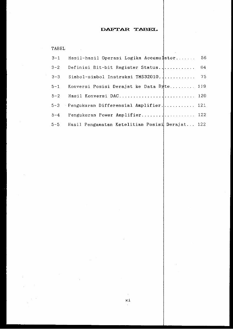
DAF-rAR TABEL
TABEL
3-1 Hasil-hasil Operasi Logika Accumu ator....... 56
3-2 Definisi Bit-bit Register Status............. 64
3-3 Simbol-simbol Instruksi TMS32010. . . . . . . . . . . . 75
5-1
5-2
5-3
5-4
5-5
Konversi Posisi Derajat ke Data B te ......... 119
Hasil Konversi DAC .............. . 120
Pengukuran Differensial Amplifier ............ 121
Pengukuran Power Amplifier ................... 122
Hasil Pengamatan Ketelitian Posis Derajat ... 122
xi
BAB I
PENDAHULUAN
I.l LATAR BELAKANG
Sistem kontrol otomatik sudah tid k asing lagi
dalam dunia teknologi, baik teknologi el. ktronik maupun
yang non-elektronik, karena kontrol otomatik mem-
berikan kemudahan dalam pengaturan u sistem agar
diperoleh performansi yang sesuai.
Dengan berkembangnya teknologi elek ronika khusus-
nya di bidang mikroelektronika dan digital, maka
sistem kontrol otomatik mulai mengara ke teknologi
digital. Juga dengan lahirnya chip-chipl mikroprosesor
yang menawarkan banyak keandalan, m rangsang para
perancang untuk beralih ke sistem ontrol dengan
mempergunakan mikroprosesor atau mikroko ter.
Dalam sistem kontrol dikenal sis em pengaturan
motor dengan kontroler PID (Proportional Integral and
Derivative). Salah satu aplikasinya ada ah pada peng-
aturan posisi be ban mekanik yang sesuai dengan .posisi
acuannya, a tau dikenal dengan isme posisi.
Dengan pengaturan ini diharapkan akan ke-
luaran sistem yang tepat, stabil, dan me unyai respon
yang cepat untuk mencapai kondisi yang d kehendaki.
_./
!.2 PERKASALAHAN
Pada sistem kontrol PID analog bi diimple-
mentasikan dengan menggunakan penguat op asi (OP-AMP)
1
2
atau dengan rangkaian transistor diskri . Dalam tugas
akhir ini fungsi dari OP-AMP atau trans"stor tersebut
digantikan oleh chip prosesor sinyal di ital TMS32010
dengan beberapa perangkat tambahannya. ersamaan yang
ada pacta sistem kontrol PID ditulis dalam suatu
program (software) sehingga eluruhan alat
ini dapat berfungsi sebagai penggant sistem PID
analog. Dengan cara di atas diharapkan respon sistem
menjadi lebih baik dibandingkan de n pengaturan
secara analog.
!.3 PEMBATASAN PERMASALAHAN
Titik berat pembahasan dalam tu as akhir ini
adalah implementasi dari prosesor s nyal digital
TSM32010, suatu chip prosesor khusus memiliki 16
bit bus data dengan kemampuan 4 K word ogram memori.
Prosesor tersebut bersama-sama d perangkat
tambahan lainnya mengatur sudut putar m tor DC sesuai
I .
sudut referensi yang diberikan. ebaga1 dengan sensor
posisi digunakan transduser putaran ke t berupa
potensiometer linier yang dikopel dengan pores motor.
!.4 METODOLOGI
Sebagai Jangkah pertama dalam per sistem
adalah menentukan diagram blok sistem p posisi
yang sesuai. Dari diagram blok tersebut 1 kemudian di-1
realisasikan ke bentuk rangkaian. Pacta l I kah ini akan
3
menghadapi ban yak pilihan untuk entukan tipe
rangkaian maupun jenis komponen ya akan dipakai
agar diperoleh spesifikasi yang sesuai.
Langkah selanjutnya, membuat alih sistem
kontol PID. Langkah ini dilakukan i cara pen-
dekatan analog, yaitu menentukan fungsi lih dari rang-
kaian PID analog kemudian mengkonversik nya ke bentuk
mikroprosesor. Dalam hal ini fungsi al h dari motor
diabaikan.
Dari fungsi alih yang didapat kemud an ditentukan I
koefisien-koefisien yang diperlukan. enentuan ko-
efisien ini dilakukan dengan cara menco a-coba hingga
diperoleh koefisien yang tepat, artinya keluaran dari
sistem berupa sinyal redaman kritis(crit cal damp) dan
tidak terjadi osilasi. Dengan bantuanl komputer IBM
PC/XT besarnya koefisien dan instruksi-i struksi untuk
menjalankan prosesor TMS32010 diisikan ke dalam RAM
statik yang berfungsi sebagai memori p ogram melalui
teknik interface.
1.5 LANGKAH-LANGKAH PEKBAHASAN
Bab II Pada bab ini akan dijelaskan teori
yang menunjang dalam perencan dan pem-~
buatan sistem pengaturan posis dengan motor
DC. Di sini meliputi teori kontrol
PID, prinsip kerja motor searah dan I
prinsip-prinsip pengaturannya I serta kom-
4
ponen-komponen penunjang lain
Bab III Pada bab III khusus akan bahas mengenai
prosesor sinyal digital TMS32 10.
Bab IV Pada bab ini akan dibahas langkah-langkah
perencanaan dan pembuatan si pengaturan
posisi dengan motor DC, liputi sistem
dekoding memori maupun I/0 d sistem yang
akan dibuat, rangkaian ADC an DAC, rang-
kaian transduser serta rangka penguat daya
untuk penggerak motor.
Bab v Bab ini berisi ten tang penguj yang
dibuat dan hasilnya dibandin kan dengan pe
rencanaan semula.
Bab VI Pada bagian ini akan diber kesimpulan
dari keseluruhan perencanaan dan pembuatan
sistem serta beberapa saran
BAB II
'T'EORI PHNUNJ .............. _
II.l PENDAHULUAN
Dalam bab II ini akan dibahas tent
teori yang menunjang dalam perencana
aturan posisi dengan motor DC yang
prosesor sinyal digital sebagai
utama.
Mula-mula akan dibahas tentang
PID dalam sistem analog serta pendeka
digital untuk nantinya diimplementasik
dalam bentuk program. Dilanjutkan
tentang prinsip kerja motor DC dan
aturannya. Dan terakhir akan dibahas
konversi data yaitu konversi DAC dan AD
II.2 KONTROLER PID DIGITAL
dasar-dasar
sistem peng-
pengendali
kontrol
nya ke bentuk
proses or
pembahasan
a-cara peng
proses
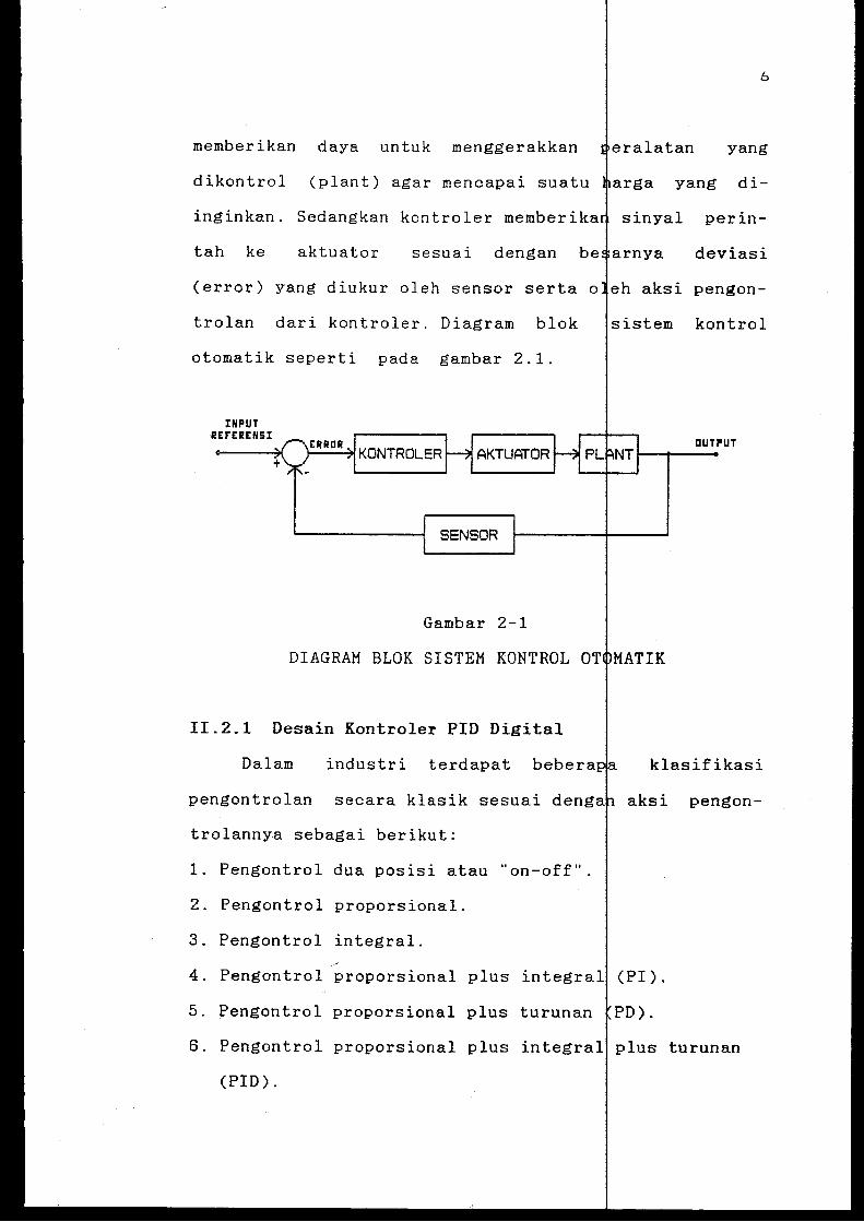
Prinsip kontroler otomatik adal membandingkan
harga output sistem terhadap suatu referensi,
menentukan deviasi dan menghasilkan kon-
trol yang akan memperkecil deviasi nol atau
sampai suatu harga yang terkecil. Cara troler otoma-
tik menghasilkan sinyal kontrol disebut sebagai aksi
pengontrolan lcontrol action).
Sistem kontrol otomatik pada umumny terdiri dari
empat bagian utama: sensor, kontroler, aktuator dan
plant. Sensor mengukur perilaku dari s stem. Aktuator
5
6
memberikan daya untuk menggerakkan ralatan yang
dikontrol (plant) agar mencapai suatu rga yang di-
inginkan. Sedangkan kontroler memberik sinyal perin-
tah ke aktuator sesuai dengan deviasi
(error) yang diukur oleh sensor serta o eh aksi pengon-
trolan dari kontroler. Diagram blok
otomatik seperti pada gambar 2.1.
INPUT RErERENSI
AKTUATOR
SENSOR
Gambar 2-1
sistem kontrol
DUTPUT
DIAGRAM BLOK SISTEM KONTROL OT MATIK
!!.2.1 Desain Kontroler PID Digital
Dalam industri terdapat bebera klasifikasi
pengontrolan secara klasik sesuai deng aksi pengon-
trolannya sebagai berikut:
1. Pengontrol dua posisi atau "on-off".
2. Pengontrol proporsional.
3. Pengontrol integral. /
4. Pengontrol proporsional plus integral (PI).
5. Pengontrol proporsional plus turunan PD).
6. Pengontrol proporsional plus integral plus turunan
(PID). I
7
Pada desain sistem kontrol analog ( aktu kontinyu) I
banyak digunakan kontroler PID karena ipe ini mem-
punyai kestabilan dan performansi sist m yang baik.
Diagram blok kontroler PID analog unjukkan pada
gambar 2-2. Fungsi alih dari kontroler i i adalah:
U(s)
E(s)
E(s)
- D( s) = Kp + s
Kp
Kr/s
Kos
Gambar 2-2 1 )
KONTROLER PID
Kontroler PID adalah tipe lag-le
Pada pembahasan ini tidak akan
(2.1)
compensator.
kan mengenai
compensator, namun dengan melihat gambar ode plot yang
diberikan di bawah, akan memberikan gamb an yang cukup
jelas tentang hal ini.
Pertama akan dibahas kontroler PI
plus-intergral). Fungsi alih dari
D(s) KI = Kp-+
s =
s
1) H. 6opal, 1988, Digital Control Engineering, p.137
1 +
s
proportional-
r PI adalah:
;a = Kp/KI
8
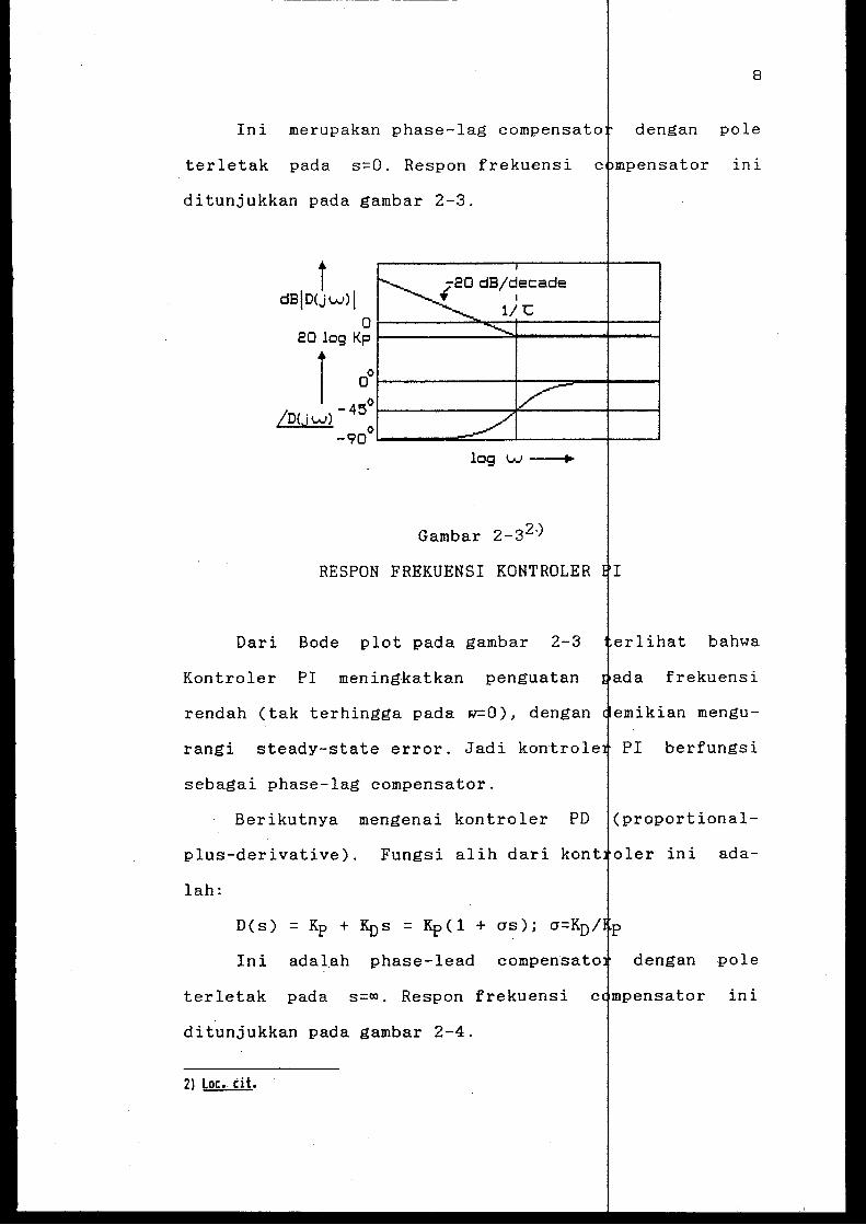
Ini merupakan phase-lag compensate dengan pole I
terletak pada s=O. Respon frekuensi c mpensator ini
ditunjukkan pada gambar 2-3.
j .{20 dB/~ecade dBj D(j w) I l/ '(;
0~------~~~+-------~----~
20log Kp~----------~--------~--~
l o:r-------+---=----f--i /D(Jw) -45
-90°~------~~--~-------4----~ log w .,
Gambar 2-32.)
RESPON FREKUENSI KONTROLER I
Dari Bode plot pada gambar 2-3 erlihat bahwa
Kontroler PI meningkatkan penguatan ada frekuensi
rendah (tak terhingga pada w=O), dengan emikian mengu-
rangi steady-state error. Jadi kontrole PI berfungsi
sebagai phase-lag compensator.
Berikutnya mengenai kontroler PD (proportional-
plus-derivative). Fungsi alih dari kont oler ini ada-
lah:
D(s) = Kp + Kos = Kp(l + as); a=Ko/
Ini adalah phase-lead compensate dengan pole
terletak pada s=oo. Respon frekuensi c ensator ini
ditunjukkan pada gambar 2-4.
2) Loc. Cit.
9
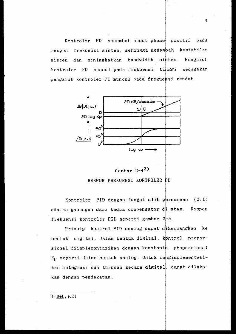
Kontroler PO menambah sudut phase positif pada
respon frekuensi sistem, sehingga men kestabilan
sistem dan meningkatkan bandwidth Pengaruh
kontroler PD muncul pada frekuensi i sedangkan
pengaruh kontroler PI muncul pada frekue si rendah.
j 20 dB/~ec:ade-. dBID(j W) I 1/ t:
0~-----------r~~--~r---~ 20logKp~----------~~----~r---~
1 90°1----------+---=---~-----l 45° /D(J w) 1--------,1'-----+---1
00~------~~--~--------+---~ log w ..
Gambar 2-43 )
RESPON FREKUENSI KONTROLER
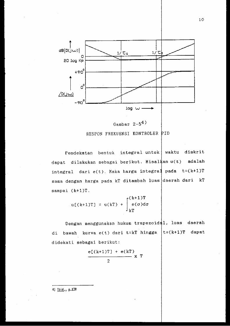
Kontroler PID dengan fungsi alih rsamaan (2.1)
adalah gabungan dari kedua compensator atas. Respon
frekuensi kontroler PID seperti gambar
Prinsip kontrol PID analog dapat kembangkan ke
bentuk digital. Dalam bentuk digital, trol proper-
sional diimplementasikan dengan konstant proporsional
Kp seperti dalam bentuk analog. implementasi
kan integrasi dan turunan secara digital dapat dilaku-
kan dengan pendekatan.
3) Ibid., p.138
i dBIDUw>l
0~------~~~~--------~+-~~------~ 20logKp~--------~~----------~~----------~
/D(jw)
log w "'
Gambar 2-54 )
RESPON FREKUENSI KONTROLER ID
10
Pendekatan bentuk integral untuk waktu diskrit
dapat . I
dilakukan sebagai berikut. M1sal an u(t) adalah
integral dari e(t). Maka harga integra pada t=(k+l)T
sama dengan harga pada kT ditambah luas daerah dari kT
sampai ( k+ 1 )T.
( k+l )T
u[(k+l)T] = u(kT) + J e(cr)dcr kT
Dengan menggunakan hukum trapezoid 1, luas daerah
di bawah kurva e(t) dari t=kT hingga t=(k+l)T dapat
didekati sebagai berikut:
e[(k+l)T] + e(kT) X T
2
4) Ibid., p.139
11
Jadi:
T u[(k+l)T] = u(kT) + {e[(k+l)T] e(kT)} (2.2)
2
Dengan transformasi-z, kita dapatkan:
T zU(z) = U(z) + [ zE ( z) + E z)]
Maka: U(z)
E(z) =
T
2
2
[
z +
z -(2.3)
Jadi Persamaan (2.3) adalah fungsi alih untuk integra-
tor diskrit.
Selanjutnya mengenai pendekatan bentuk turunan
untuk waktu diskrit. Jika turunan dari e(t) pada t=kT
adalah u(kT), maka:
u(kT) :::::
Jadi:
e(kT) - e[(k-l)T]
T
U(z) (z - 1) = (2.4)
E(z) Tz
Sebenarnya banyak cara yang dapat ilakukan untuk
pendekatan waktu diskrit pada integra dan turunan.
Namun dalam pembahasan ini akan di persamaan
(2.3) untuk integral dan (2.4) untuk Diagram
blok Kontroler PID digital ditunjukkan ada gambar 2-6.
Metoda konversi dari U(z)/E(z) = D(z) jadi algoritma
numerik akan dibahas pada bagian beriku nya.
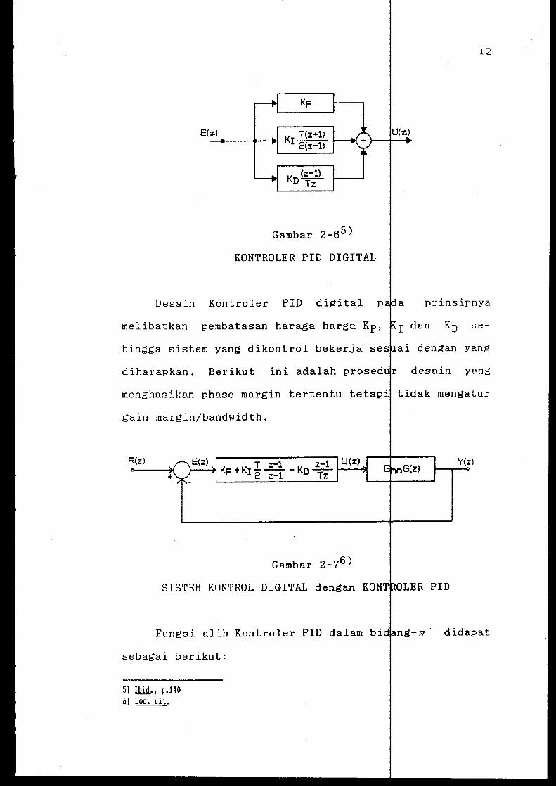
E(z:)
Kp
KI T(z+1) 2(:::-1)
(z-1) Ko Tz
Gambar 2-65 )
KONTROLER PID DIGITAL
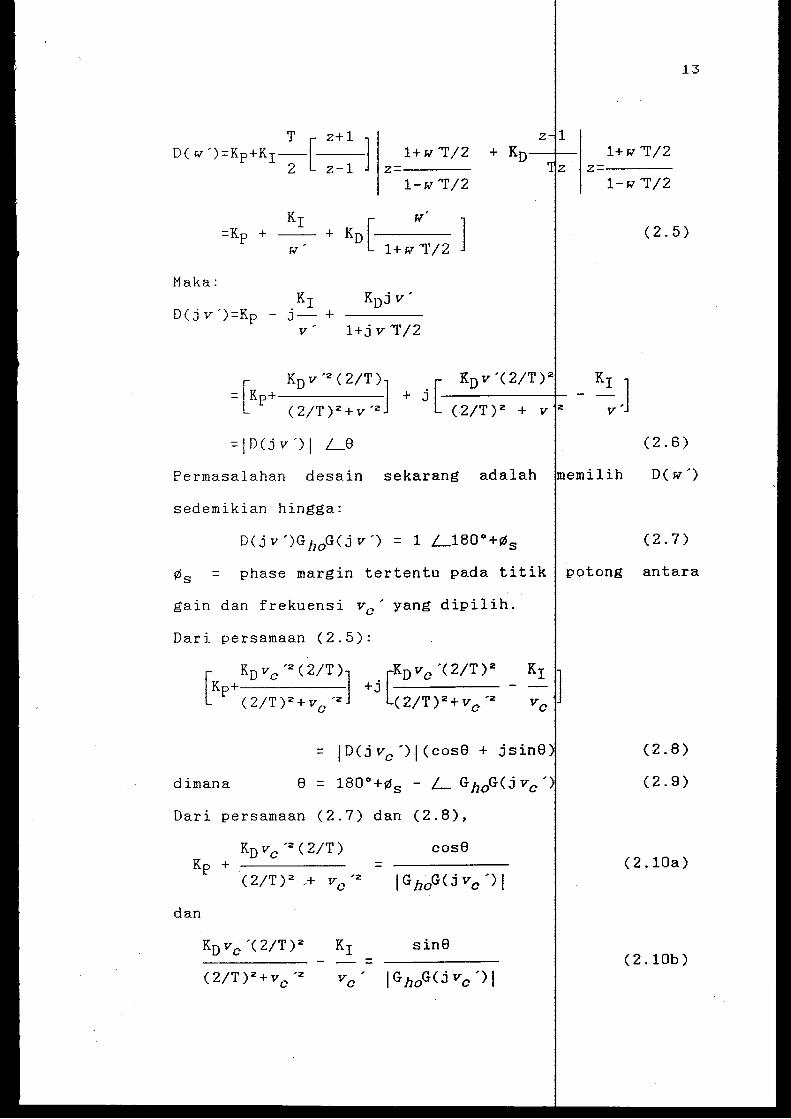
Desain Kontroler PID digital
12
a prinsipnya
melibatkan pembatasan haraga-harga Kp, I dan KD se
hingga sistem yang dikontrol bekerja se ai dengan yang
diharapkan. Berikut ini adalah prosed desain yang
menghasikan phase margin tertentu tetap tidak mengatur
gain margin/bandwidth.
R{z)
Gambar 2-76 )
SISTEM KONTROL DIGITAL dengan
Fungsi alih Kontroler PID dalam b
sebagai berikut:
5) Ibid., p.140 b) Loc. cit.
Y{z)
ER PID
didapat
13
T z+1 D( w ')=Kp+K1-
2-[ ] l+w 'T/2 + Ko--1--
z-1 z l+w'T/2
z 1-w'T/2 1-w'T/2
=Kp + w'
+ K0 [ ] l+w'T/2 w
(2.5)
Maka: K1 Koj v'
D(j v ')=Kp - j- + v 1+jv'T/2
= [Kp+ Ko v '2
( 2/T )] + j [-K_o_v_'<_2_1_T_)-II
( 2/T ) 2 + v ' 2
=I D ( j v , ) I L8 (2.6)
Permasalahan desain sekarang adalah emilih D( w ')
sedemikian hingga:
(2.7)
¢s = phase margin tertentu pada titik potong antara
gain dan frekuensi v 0 ' yang dipilih.
Dari persamaan (2.5):
dimana
- ID(jv0 ')1(cos8 + jsin8
8 = 180°+¢8 - L Gh0 G(j v 0 '
Dari persamaan (2.7) dan (2.8),
cos8 =
dan
sine =
(2.8)
(2.9)
(2.10a)
(2.10b)
14
Persamaan (2.9) dan (2.10) adalah amaan desain.
Persamaan-persamaan ini juga berla untuk desain
kontroler PI dan PD dengan penguatan (Ko atau KI)
diberi harga nol.
Untuk Kontroler PI,
cosS Kp = (2.11a)
sinS = (2.11b)
Untuk suatu plant Gh0 G(w') u, pemilihan
v0
' dan ¢5
akan menentukan harga I .
Untuk Kontroler PD, persamaan (2.1 ) didapat:
[ sinS ] [ (2/T)'+vc
Ko = IGhoG(jvc ')I v
0 '(2/T)
cosS Ko v c ' 2 ( 2/T )
Kp = IGhoG(jvc')l (2/T) 2 + v 0
Kedua konstanta Kp dan Ko yang
bisa diperoleh untuk plant Gh0 G(w')
memilih harga v0
' dan ¢ 5 tertentu.
Pada Kontroler PID, tidak ada
]
diketahui
tentu, dengan
ur yang seder-
hana untuk menyelesaikan persamaan (2. ) untuk Kp,Kr
dan K0 . Akan tetapi, jika v 0 '<<2/T,
dapat direduksi menjadi:
Kr = Kp + -- + Ko w'
w
rsamaan (2.5)
= [ Kp ' + ~ l ( Kp" + Ko (' • ) (2.12)
v Bagian PI
15
Dengan demikian teknik desain pada Kontroler PID
dapat dilakukan dengan mengikuti teknik desain untuk
Kontroler PI dan Kontroler PD.
II.2.2 Realisasi Fungsi Alih Pulsa
Pada bagian sebelumnya telah ahas mengenai
prosedur-prosedur yang menghasilkan alg ritma kontrol
dalam bentuk fungsi alih pulsa. Jika fu gsi alih ini
disusun ke dalam rumus state diagram ata state space,
akan dapat secara langsung diprogram ada komputer.
Pada bagian ini akan dibahas mengenai re lisasi fungsi
alih pulsa ke dalam state model.
Fungsi alih rasional H(z) dapat dir alisasi dengan
suatu state model time-invariant dimens I
linier ter-
hingga bila dan hanya bila H(z) adalah suatu pecahan
yang bisa diselesaikan. Derajat polino ial pembilang
adalah kurang dari atau sama dengan pol nomial penye-
but.
Jika fungs~ alih pulsa H1 (z) adalah:
bozn + b1zn-1 + + bn H1(z) = =
zn + a1zn-1 + + ~ (2.13)
Bentuk ini dapat dinyatakan dalam state model dengan
bentuk:
x(k) = Fx(k-1) + gu(k-1) (2.14a) ~
Y1 (k) = cx(k) + du(k) (2.14b)
dimana F adalah matriks konstan nxn, g I adalah vektor I I
konstan nx1, c adalah vektor konstan 1x dan d adalah
konstanta skalar.
16
Dari persamaan (2.13) jelas bahwa j ka harga poli-
nomial pembilang lebih besar daripada po inomial penye-
but, maka perluasan H1(z) ke dalam
mengandung harga positif dalam z
'prediksi', yaitu output mendahului inpu
tan -1 z akan
g menunjukkan
Dengan menggunakan pembagian yang anjang, H1 (z)
pada persamaan (2.13) dapat ditulis seb ai:
13 n-1 + 13 n-2 + + l3n 1z 2z ... H1(z) = + bO (2.15a)
zn + a1zn-1 + ... + an
N(z) = (2.15b)
.6(z)
Dari persamaan (2.14) dan (2.15) dengan mudah
diketahui bahwa d = b 0 . Dengan bagian t ansmisi lang
sung dari state model yang telah didapa , maka untuk
selanjutnya fungsi rasional di atas menj i:
13 n-1 + 13 n-2 + + l3n lz 2z ... H(z) =
zn + alzn-1 + ... + ~
sehingga fungsi alih ini dapat
state model dengan bentuk:
x(k) = Fx(k-1) + gu(k-1)
y(k) = cx(k)
= (2.16)
ke dalam
(2.17a)
(2.17b)
Pada persamaan (2.16) derajat polin ial pembilang
adalah (n-1). Jika derajatnya kurang i (n-1), maka
hasil yang d~dapat bisa langsung d unakap dengan
memberikan harga koefisien 13 1 sama denga nol.
Di sini juga akan digunakan nguatan Mason
untuk grafik aliran sinyal yang ungkan fungsi
17
alih dengan grafik aliran sinyal (signa flow graph).
Rumus ini menyatakan,
1 H( z) -
dimana
Pk = penguatan lintasan maju ke-k
~ = determinan grafik
= 1- (jumlah semua penguatan loop
(jumlah hasil kali penguatan dari
yang mungkin dari dua loop yang ti
an) (jumlah hasil kali penguat
kombinasi yang mungkin dari tiga 1
bersentuhan) +
~k = kofaktor dari determinan
dengan menghilangkan loop-loop
lintasan maju ke-k.
Misalkan pada persamaan(2.16) diambil n
Y(z)
U(z) = H(z) -
Ini merupakan fungsi alih order-tiga, se
tiga state variable x1 , x2 dan x3.
mempunyai tiga unit penunda z- 1 .
Persamaan (2.19) juga dapat disusun seb
H(z) ( -1 1- -a.1 z
Dengan membandingkan persamaan
diketahui bahwa grafik aliran sinyal
(2.20) terdiri dari:
(2.18)
berbeda) +
a kombinasi
bersentuh-
dari semua
yang tidak
maju ke-k
menyentuh
(2.19)
akan
(2.20)
dan ( 2.18),
persamaan
18
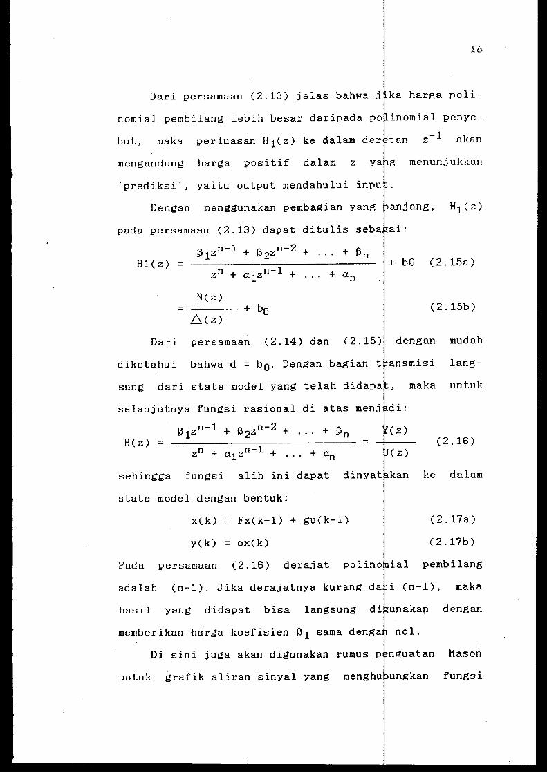
(i) tiga loop umpan balik (saling bersen uhan) dengan
gain
(ii) tiga lintasan maju yang '
mempunyai penguatan
h loop
a -3 ~3z .
dan
Konfigurasi grafik aliran sinyal (S1 ate diagram)
I
yang memenuhi syarat untuk ini ditunjukk pada gambar
2-8. Dengan mengambil output
state variable, akan didapat
X 1 ( k) = -a 1x 1(k-1) + x2(k-1)
x 2< k) = -a2x 1 ( k-1) + x 2(k-1) + ~
x 3( k) = -a 3x 1 (k-1) + ~ 3u( k-1)
y(k) = x 1 (k)
Gambar 2-87 )
STATE DIAGRAM UNTUK PERSAMAAN
unda sebagai
k-1)
k-1)
Y(z)
(2.21)
II.2.3 Realisasi Fungsi Alih Kontroler ID Digital
Berdasarkan teori yang telah dibah bag ian
II.2.2 dan dengan memperhatikan diagram Kontroler
7) Ibid., p.197
19
PID pada gambar 2-6, maka fungsi alih Kontroler PID
Digital ben uk I
dapat diselesaikan dalam algoritma
numerik.
Dari diagram blok pada gambar 2-6, fungsi alih
Kontroler PID digital adalah:
U(z) T -- = Kp + Kr-E(z) 2
a tau
[~] z-1
1 + Ko
T
U(z) T -1
[ l+z ] -- = Kp + Kr-1 -1 -z E(z) 2
= ------------------~--------------~---1-z-1
=
bila
Maka:
[Kp+Kr(T/2)+KofTJ + [Kr(T/2)-Kp-2(Ko/T)]z 1 + (KoJT)z-2
1-z-1
K1 - Kp+Kr(T/2)+Ko/T,
K2 = Kr(T/2)-Kp-2(Ko/T) dan
K3 = Ko/T
U(z) z-1 + K -2 K1 + K2 3 z = (2.22)
-1 E(z) 1 - z
Persamaan (2.22) merupakan fungsi lih order dua
dan mempunyai state variable x 1 dan x2. Grafik aliran
sinyal seperti gambar 2-9.
Dari gambar 2-9 diperoleh:
(a.) x 1(k) = x 1(k-1) + x 2(k-1) + K1 e(k
(b.) x 2(k) = K2 e(k) + K3 e(k-1), atau 1
x2(k-1) = K2 e(k-1) + K3 e(k-2)
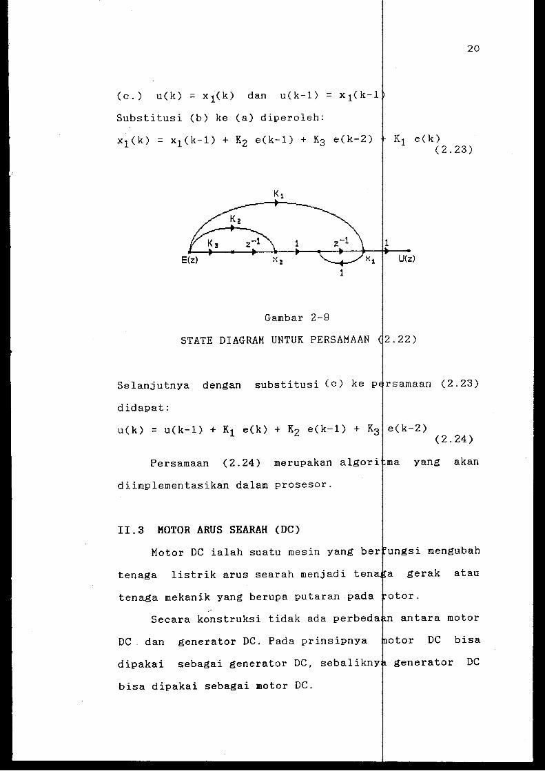
(c.) u(k) = x 1(k) dan u(k-1) = x 1(k-1
Substitusi (b) ke (a) diperoleh: I
1
20
K1 e(k) (2.23)
x 1 U(z)
1
Gambar 2-9
STATE DIAGRAM UNTUK PERSAMAAN 12.22)
Selanjutnya dengan substitusi (c) ke P rsamaan (2.23)
didapat:
u(k) = u(k-1) + K1 e(k) + K2 e(k-1) + K3 e(k-2) (2.24)
Persamaan (2.24) merupakan algori ma yang akan
diimplementasikan dalam prosesor. I
II.3 MOTOR ARUS SEARAH (DC)
Motor DC ialah suatu mesin yang ber ungsi mengubah I
tenaga listrik arus searah menjadi ten gerak atau
tenaga mekanik yang berupa putaran pada
Secara konstruksi tidak ada perbeda antara motor
DC . dan generator DC. Pada prinsipnya tor DC bisa
dipakai sebagai generator DC, sebalikny generator DC
bisa dipakai sebagai motor DC.
21
!!.3.1 Prinsip Dasar Motor DC
Prinsip dasar motor arus searah ad 1ah bi1a sebuah
kawat berarus di1etakkan antara kutub m et (U-S) maka
pada kawat itu akan bekerja suatu gaya yang menggerak-
kan kawat itu.
Arah gerakan kawat sesuai dengan · kaidah tangan
kiri" yang berbunyi sebagai berikut :
"Apabila tangan kiri terbuka di1et kkan di antara
kutub Utara (U) dan Se1atan (S) ehingga garis-
garis gaya yang ke1uar dari kutub Utara menembus
i te1apak tangan kiri dan arus di da am kawat menga-
1ir searah dengan arah keempat i, maka kawat
itu akan mendapat gaya yang arahn sesuai dengan
arah ibu jari"
Besarnya gaya yang ditimbu1kan
F = B i 1 Newton (2.25)
dimana B = kepadatan f1uks magnet (satu Weber).
i - arus 1istrik yang menga1ir ( atuan Ampere).
1 = panjang kawat penghantar (sa an meter).
II.3.2 Konstruksi Motor DC
Motor arus searah mempunyai b yang diam
(stator) dan bagian yang berputar otor). Bagian
stator terdiri dari badan motor (body) yang memi1iki
1empeng-1empeng kutub magnet yang padanya.
Untuk motor keci1, 1empengan-1empengan ada1ah
magnet permanen. Sedang pada motor yan besar berupa
e1ektromagnetik. Umumnya lempengan-1e engan magnet
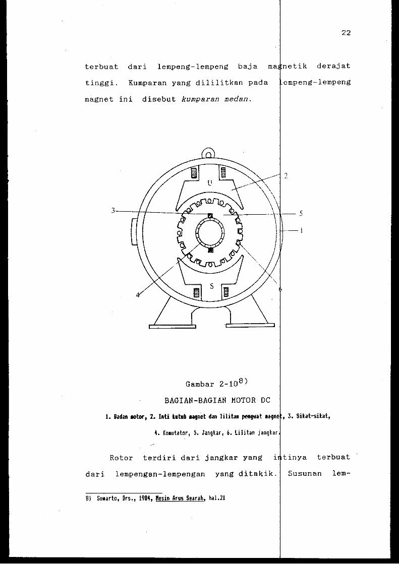
terbuat dari lempeng-lempeng baja m
tinggi. Kumparan yang dililitkan pada
magnet ini disebut kumparan medan.
Gambar 2-10 8 )
BAGIAN-BAGIAN MOTOR DC
1. Badan 10tor, 2. Inti tutub aagnet dan lilitan peDqttat
4. Koautator, 5. Jangkar, b. lilitan jangkar
22
etik derajat
empeng-lempeng
, 3. Siiat-sitat,
Rotor terdiri dari jangkar yang i tinya terbuat
dari lempengan-lempengan yang ditakik. Susunan lem-
8) Suaarto, Drs., 1984, "esin Arus Searah, hal.21

23
pengan-lempengan membentuk celah-cel h. Konduktor
kumparan jangkar dimasukkan pada celah-c lah tersebut.
Ujung dari tiap-tiap kumparan dihubung pada satu
segmen Komutator. Tiap segmen merupakan pertemuan dua
ujung kumparan yang terhubung ke segmen tu. Gambar 2-
10 menunjukkan bagian-bagian motor DC.
II.3.3 Torsi Motor
Bila kumparan medan diberi tegang maka akan
terbentuk kutub-kutub magnet utara dan selatan pada
lempeng-lempeng magnet. Pada kumparan jangkar juga
diberi tegangan melalui komutator dan si at-sikat. Hal
ini menyebabkan terbentuknya medan magne di sekeliling
masing-masing konduktor. Maka akan meng silkan torsi
seperti tampak pada gambar 2-11.
DIRECTION OF TORQUE
Gambar 2-119)
STATOR FIELD
TORSI PUTAR PADA MOTOR DC
9) Joe Kaiser., 1982, Electrical Power, p. 209
24
Torsi total yang dihasilkan oleh gaya magnetik
dari kedua medan sebanding dengan:
1. Kuat medan, ¢.
2. Arus jangkar, Ia.
Persamaannya adalah:
T = K x ¢ x Ia
dengan: T = torsi I = arus a
(2.26)
¢ = kuat medan K = ta desain
II.3.4 Hubungan-hubungan yang Berlaku DC
Pada motor DC berlaku hubungan-hu
(2.27)
dengan I a = arus jangkar
v = tegangan sumber
Eb = ggl lawan dari jangkar
Ra = tahanan lilitan jangkar
p
Eb = ¢ z N (-) (2.28) a
dengan
¢ = besarnya fluks magnet tiap kutub
Z = jumlah kawat penghantar pada lili an jangkar
N = kecepatan putar motor (rpm)
P = jumlah kutub
a = jumlah cabang paralel lilitan jan kar i
Tegangan V selalu berlawanan arab engan ggl lawan
sedang pada jangkar terdapat tegan an jatuh yang I
disebabkan oleh lilitan jangkar yang m mpunyai res is-
25
tansi Ra. Tegangan jatuh itu sebesar IaR . Jadi
I
Dari bentuk ini dapat dituliskan
V Ia = Ebia + IazRa
dengan
v I a = day a listrik yang masuk ke
Ebia = day a mekanik yang setara
listrik yang timbul dalam j
Ia2Ra = rugi tembaga dalam jangkar
II.3.5 Jenis-jenis Motor DC
Berdasarkan sumber arus penguat m
DC dapat dibedakan atas
- Motor DC penguat terpisah
(2.29)
(2.30)
j gkar
day a
kar = Pm
etnya, motor
arus penguat medan magnet dipero h dari sumber
DC diluar motor.
- Motor DC penguat sendiri :
arus penguat medan magnet berasa dari motor itu
sendiri.
Berdasarkan hubungan lilitan guat magnet
terhadap lilitan jangkar motor DC dibed
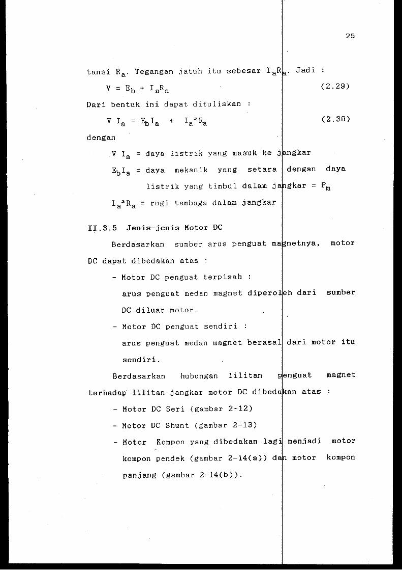
- Motor DC Seri (gambar 2-12)
- Motor DC Shunt (gambar 2-13)
- Motor Kompon yang dibedakan menjadi motor
kompon pendek (gambar 2-14(a)) d motor kompon
panjang (gambar 2-14(b)).
OC: POWER SOURC:E
~(--I
5Eii!IES f'IELO C:OIL
ARMATURE
Gambar 2-12 10 )
RANGKAIAN PENGGANTI UNTUK MOTOR C SERI
I ) Ifl
Ia --7
+ OC: POWEll SHUNT ARMATURE
SUPPLV riELO
Gambar 2-13 11 )
RANGKAIAN PENGGANTI UNTUK MOTOR
SHUNT F'IELO
(a)
~
Gambar 2-14 12 )
SHUNT f'IELO
RANGKAIAN PENGGANTI UNTUK MOTOR
10) Ibid., p. 210 111 Ibid., p. 212 12) Ibid., p. 215
SHUNT
KOMPON
26
27
II.3.6 Motor DC Sebagai Motor Servo
Dalam sistem servomekanisme yang ggunakan motor
servo DC, konstruksi dasar motor biasan dengan
motor DC shunt yang umum. Perbedaannya terletak
pada cara menghubungkan kumparan jangk
medan terhadap sumber tegangan.
kedua kumparan dihubungkan secara paral
dan kumparan
DC shunt
dan diberi
tegangan dari sumber yang sama, tetapi p a motor servo
kumparan-kumparannya diberi tegangan da sumber yang
terpisah. Jadi motor servo sebenarn menggunakan
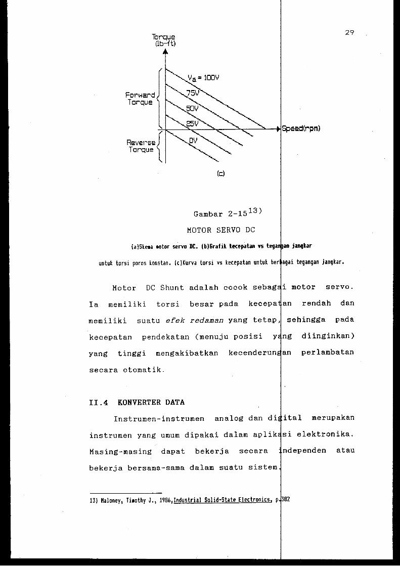
penguat terpisah. Hal ini ditunjukkan p a gambar 2-15.
Untuk membalik arah putaran motor d dilakukan
dengan dua cara yaitu dengan membalik po aritas magnet
pada kumparan medan atau membalik arah arus jangkar.
Akan tetapi bukan kedua-duanya, karena yang demikian
tidak akan mengubah arah putaran motor.
Di sini tidak akan dibahas
pengaturan kecepatan motor, tapi cukup
kecepatan pada keadaan tunak dapat
mengubah vf atau va seperti ditunjukkan
15(a). Dalam sistem servo modern, u
dilakukan terhadap Va (tegangan
Hubungan antara kecepatan
state speed) dan tegangan jangkar
gambar 2-15(b) untuk torsi konstan. Pad
but terlihat bahwa hubungan keduanya men
Akan tetapi pada sistem servo kenyata
tidaklah konstan. Ia berubah saat obyek
mengenai
bahwa
dengan
gambar 2-
pengaturan
(steady
pad a
terse
linier.
motor
g dikontrol
28
mendekati posisi yang dikehendaki dan tegangan motor
berkurang. Kurva torsi-kecepatan pada t gangan jangkar
yang bervariasi ditunjukkan pada gambar 2-15(c).
Kurva tersebut menunjukkan bahwa otor servo DC
menghasilkan torsi yang lebih besar pada kecepatan
rendah daripada kecepatan tinggi untuk egangan jangkar
Va yang diberikan. Hal ini memungkinkan motor memberi-
kan percepatan pada beban (obyek yang d atur posisinya)
dari keadaan diam dalam waktu cepat. itu kurva
torsi-kecepatan menunjukkan bahwa obyek yang
diatur mendekati posisi yang diingin dan Va ber-
kurang, motor DC mampu memberikan tor balik untuk
memperlambat gerak beban jika terlalu
tinggi. Hal ini bisa terjadi karena p kondisi ini
kumparan jangkar motor mulai bekerja erti generator.
Arus pada konduktor-konduktor jangkar b rbalik arah dan
arus balik ini menimbulkan torsi balik.
Field + v.linding
vf ?
Armature v.linding
(a)
+ Va
Steady State ' Speed (rpm)
(b)
Torque (lb-ft)
Fer' ward Torque
Reverse Torque
(c)
Gambar 2-15 13 )
MOTOR SERVO DC
untuk torsi poros ionstan. (c)Kurva torsi vs kecepatan untuk
Motor DC Shunt adalah cocok seb
29
tegangan jangkar.
servo.
Ia memiliki torsi besar pada kecepa an rendah dan
memiliki suatu efek redaman yang tetap sehingga pada
kecepatan pendekatan (menuju posisi diinginkan)
yang tinggi mengakibatkan kecenderun perlambatan
secara otomatik.
II.4 KONVERTER DATA
Instrumen-instrumen analog dan ital merupakan
instrumen yang umum dipakai dalam aplik si elektronika.
Masing-masing dapat bekerja secara ndependen atau
bekerja bersama-sama dalam suatu sistem
131 Maloney, Tiaothy J., 1986,Industrial Solid-State Electronics, p
30
Dalam dunia analog, sinyal bekerja ecara kontinyu
yang bervariasi antara jangkauan batas tas dan batas
bawah. Tetapi sinyal-sinyal pada r kaian digital
bekerja secara diskrit yang berupa retan keadaan
yang dinyatakan dengan logika "0" dan "1
Konverter data adalah suatu r ngkaian a tau
peralatan yang mengubah sinyal dari ben uk asalnya ke
besaran lain yang harganya sebanding. Mi alnya digital
to analog converter (DAC) mengkonversi word digital
yang terdiri dari bit-bit bilangan te tentu menjadi
tegangan atau arus yang mewakili harga ilangan biner
dari word digital tersebut. Hisalnya DA 8-bit meng-
hasilkan sinyal output 0 volt bila inputnya di-
berikan harga biner 000000002 dan hasilkan 2,56
volt bila diberikan input 111111112 . untuk setiap
harga biner yang diberikan, maka akan di asilkan harga
output yang sebanding.
Analog to digital converter (ADC) alah kebalikan
dari DAC yaitu mengkonversi sinyal log (tegangan
atau arus) menjadi word biner yang seban ing.
Konverter data terutama banyak igunakan pada
aplikasi interface suatu tranduser
digital atau input komputer; dan interf
peralatan
output
suatu instrumen digital dengan perangkat analog seperti
motor, alat ukur analog dan lain-lain.
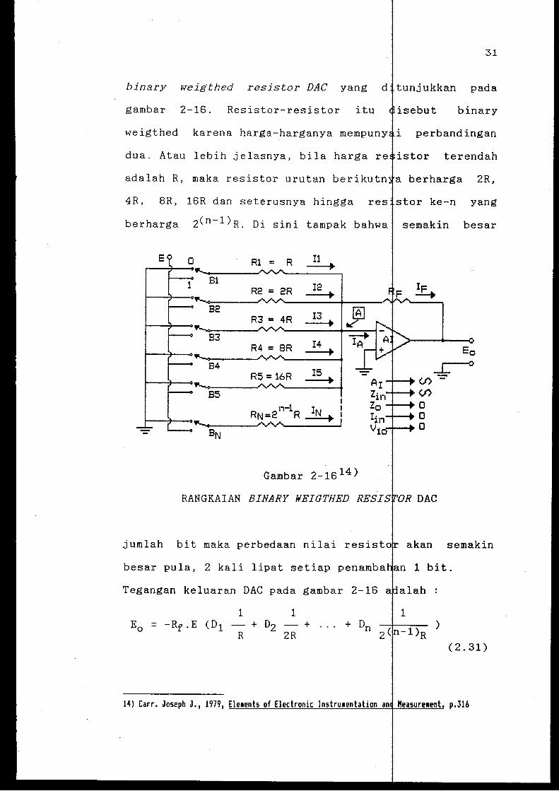
!!.4.1 Rangkaian Dasar DAC
Rangkaian dasar DAC yang paling mudah adalah
31
binary weig'thed .r·esistor DAC yang d tunjukkan pada
gambar 2-16. Resistor-resistor itu isebut binary
weigthed karena harga-harganya mempuny i perbandingan
dua. Atau lebih jelasnya, bila harga re istor terendah
adalah R, maka resistor urutan berikutn a berharga 2R,
4R, 8R, 16R dan seterusnya hingga res stor ke-n yang
berharga 2(n- 1 )R. Di sini tampak bahwa semakin besar
Rl = R I1 ____.. Bl
I2 R2 = 2R ----+ B2
!3 R3 = 4R ----+ B3
I4 R4 = SR ----+ B4
IS RS = 16R ----+ B5
RN=2li-1R ~ .A,.A...A.
Gambar 2-16 14 )
Eo __r:-----0
-+--.(f) -__ -!-... (f)
-t---fl' 0 -t---fl' 0
........ - ... 0
jumlah bit maka perbedaan nilai resist akan semakin
besar pula, 2 kali lipat setiap penamb 1 bit.
Tegangan keluaran DAC pada gambar 2-16
1 1 + D2 + ... + Dn
R 2R (2.31)
32
dengan D1 s/d Dn menyatakan keadaan s klar, membuka
berarti dan 0 dan menutup berarti 1. D1 me 1
Pakan MSB
I Dn adalah LSB.
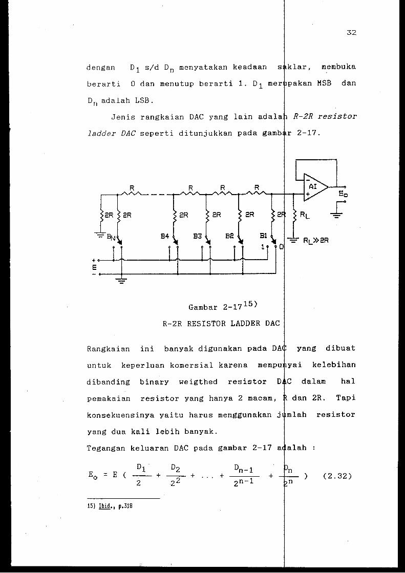
Jenis rangkaian DAC yang lain R-2R resistor
ladder DAC seperti ditunjukkan pada gamb r 2-17. I
Eo
r
Gambar 2-17 15 )
R-2R RESISTOR LADDER DAC
Rangkaian ini banyak digunakan pada D yang dibuat
untuk keperluan komersial karena kelebihan
dibanding binary weigthed resistor dalam hal
pemakaian resistor yang hanya 2 macam, dan 2R. Tapi
konsekuensinya yaitu harus menggunakan j mlah resistor
yang dua kali lebih banyak.
Tegangan keluaran DAC pada gambar 2-17
E (
15) Ibid., p.318
D . 1
2 +
Dz
z2 + ... + + (2.32)
Harga R1 >> 2R agar efek pembagi tegan
(ladder) dan R1 dapat diabaikan.
II.4.2 Rangkaian Dasar ADC
33
antara tangga
ADC adalah rangkaian yang dapat me gubah besaran
analog menjadi bentuk digital. Dengan engubahan ini
maka sinyal analog dapat diproses digital,
misalnya dengan komputer. Ada beberapa cam rangkaian
ADC yaitu :
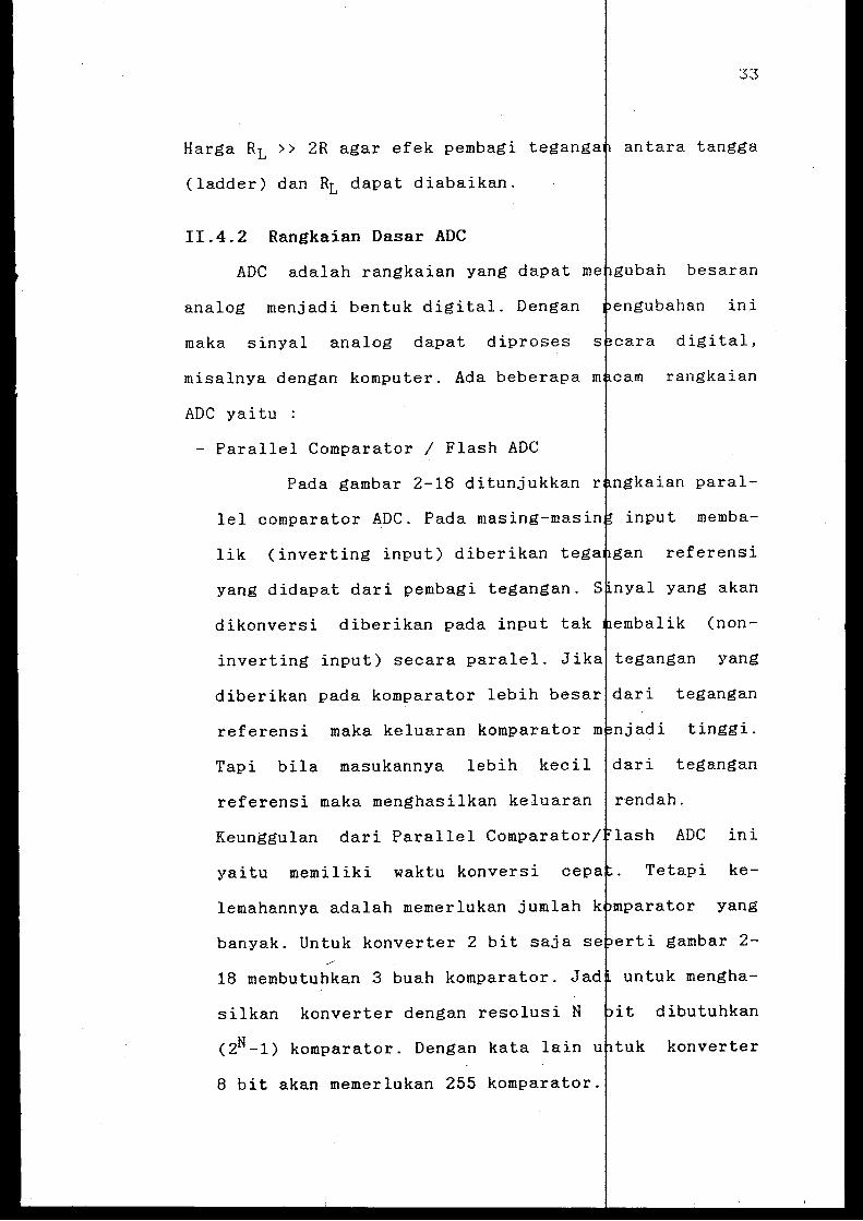
- Parallel Comparator I Flash ADC
Pada gambar 2-18 ditunjukkan r paral-
lel comparator ADC. Pada masing-masin input memba-
lik (inverting input) diberikan teg referensi I
yang didapat dari pembagi tegangan. S nyal yang akan
dikonversi diberikan pada input tak alik (non-
inverting input) secara paralel. Jika tegangan yang
diberikan pada komparator lebih besar dari tegangan
referensi maka keluaran komparator njadi tinggi.
Tapi bila masukannya lebih kecil dari tegangan
referensi maka menghasilkan keluaran rendah.
Keunggulan dari Parallel Comparator lash ADC ini
yaitu memiliki waktu konversi Tetapi ke-
banyak. Untuk konverter 2 bit saja s erti gambar 2-
silkan konverter dengan resolusi N
(2N-1) komparator. Dengan kata lain
8 bit akan memerlukan 255 komparator.
it dibutuhkan
tuk konverter
Gambar 2-18 16 )
t---+-01
CODE OUTPUT
I--+- DO
34
RANGKAIAN PARALLEL COMPARATOR/FL H ADC
- Successive Approximation ADC
ADC jenis ini banyak dipakai aplikasi
interface dengan komputer karena unyai waktu
konversi cepat disamping dapat dibuat jumlah
bit yang banyak/resolusi tinggi. lain yang
dianggap menguntungkan adalah kecepat konversinya
tidak bergantung pada besarnya tegan sinyal yang
dikonversi. Dengan kata lain konversinya
konstan.
ADC ini dibentuk dari beberapa komponen yaitu
DAC, komparator dan beberapa register erta rangkai-
an kontrol _seperti tampak pada gambar 2-19.
Konversi dilakukan dengan cara membandingkan
tegangan input analog terhadap tegang output yang
p.325
35
dihasilkan oleh ADC. Input DAC diatu oleh regis-
konversi dapat diambil dari register tput.
Cl~ck
Start --____..;~
Eo
DIAGRAM BLOK
Successive Approximation R gister
Digital-to-Analog Converter
Gambar 2-19 17 )
ION ADC
EOC
Konversi dimulai dengan sinyal
input 'start conversion'. Adanya start ini
mengakibatkan input DAC dibuat sehin MSB = '1'
dan bit-bit yang lain '0'. Output (1/2 skala
penuh) dibandingkan dengan output log yang akan
dikonversi. Bila tegangan output lebih kecil
maka bit MSB tetap '1' sedangkan output DAC
leb ih besar maka MSB m.enj ad i '0' . bit
berikutnya (1 bit lebih rendah dari ) dibuat ' 1 '
dengan keadaan MSB tetap dipertahan . Kondisi bit-
17) Joseph J. Carr., Op. cit., p.326
36
bit pada input DAC yang ada sekarang kan menghasil
kan output analog dan dibandingka lagi dengan
tegangan input untuk menentukan apa ah bit kedua
akan diubah atau tidak. Proses di at s terus ber
langsung sampai LSB, sehingga didapat output digital
dari masukan DAC yang terakhir.
Pergeseran bit dari MSB hingga LSB dilakukan
oleh register geser yang waktunya di
clock. Jadi untuk ADC 8 bit memerluk
clock. Setelah proses konversi
pulsa
waktu 8 pulsa
maka bit
'output status' akan mengeluarkan s yal 'End of
Conversion' yang menyatakan bahwa out t digital ADC
dapat diambil sebagai besaran digital yang mewakili
tegangan input analog yang dikonversi
Jenis ADC yang lain dapat dise
antara lain :
- Single-slope dan Dual-slope ADC
integrator dan counter untuk mend
digital,
di sini
menggunakan
besaran
- Tracking ADC yang menggunakan DAC dan counter.
Kedua jenis ADC tersebut juga banyak
ukur digital yang tidak memerlukan
cepat, sedangkan untuk aplikasi
digital atau ~ pada kontrol digital
konversi cepat, kedua jenis ADC
mengingat kedua jenis ADC ini
kurang.
alat
yang
sinyal
membutuhkan
dapat dipakai
konversinya
BAB III
MIKROPB:OSESO
TMS3:2010
III.l DESKRIPSI UKUK
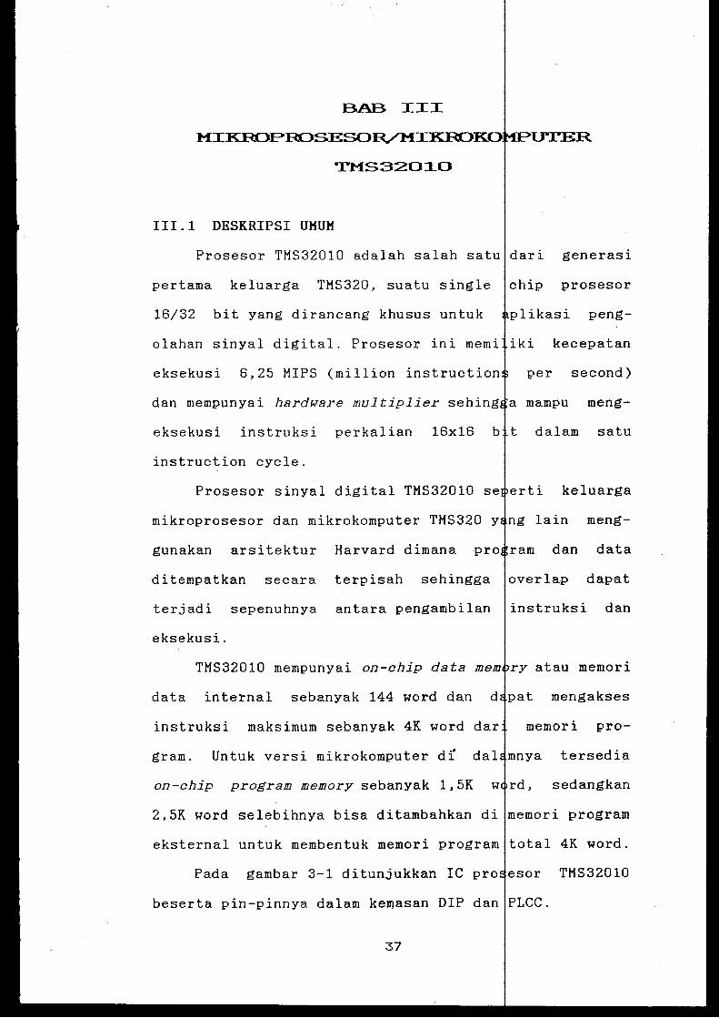
Prosesor TMS32010 adalah salah satu dari generasi
pertama keluarga TMS320, suatu single chip prosesor
16/32 bit yang dirancang khusus untuk likasi peng-
olahan sinyal digital. Prosesor ini memi iki kecepatan
eksekusi 6,25 MIPS (million instruction per second) !
!
dan mempunyai hardware multiplier sehing a mampu meng-
eksekusi instruksi perkalian 16x16 b t dalam satu
instruction cycle.
Prosesor sinyal digital TMS32010 s keluarga
mikroprosesor dan mikrokomputer TMS320 y g lain meng-
gunakan arsitektur Harvard dimana pro ram dan data
ditempatkan secara terpisah sehingga overlap dapat
terjadi sepenuhnya antara pengambilan instruksi dan
·eksekusi.
TMS32010 mempunyai on-chip data mem y atau memori
data internal sebanyak 144 word dan d mengakses
instruksi maksimum sebanyak 4K word dar 1
memori pro-
gram. Untuk versi mikrokomputer d1 dal tersedia
on-chip program memory sebanyak 1,5K sedangkan
2,5K word selebihnya bisa ditambahkan di memori program I
eksternal untuk membentuk memori program ltotal 4K word.
Pada gambar 3-1 ditunjukkan IC pro esor TMS32010 I
beserta pin-pinnya dalam kemasan DIP dan 1
PLCC.
37
AI/PAI
AOIPAO
MCIMP
iiS !NT
CLKOUT
XI
X21CLKIN
810
Vss 08
09
010
011
012
013
014
015.
07
06
(a)
A21PA2
AJ
A6
A7
AS
MEN
DEN
W£
vee A9
AIO
All
DO
01
02
03
04
05
CLKOUT
XI
X2'CLKIN 9
BtO tO
NC 11
v55 12
08 13 09 ,.
010 IS 011 012
Gambar 3-1 18 )
IC PROSESOR TMS32010
4 3 2 '44434241 0
B 19 21122324 25 2617
(b)
38
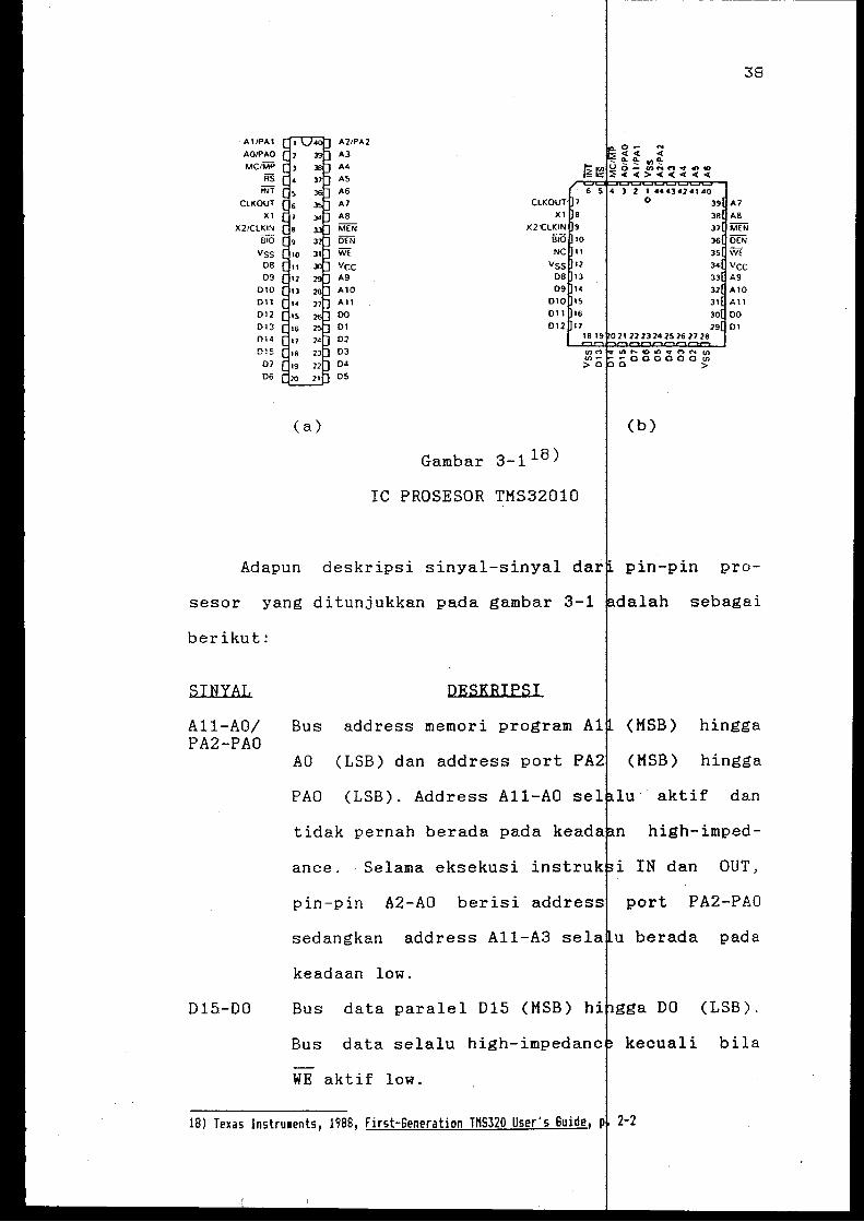
Adapun deskripsi sinyal-sinyal pin-pin pro-
sesor yang ditunjukkan pada gambar 3-1 alah sebagai
berikut:
SINYAL
A11-AO/ PA2-PAO
015-DO
DESKRIPSI
Bus address memori program A1 (MSB) hingga
AO (LSB) dan address port PA2 (MSB) hingga
PAO (LSB). Address A11-AO lu aktif dan
tidak pernah berada pada kead n high-imped-
ance. Selama eksekusi i IN dan OUT,
pin-pin A2-AO berisi address port PA2-PAO
sedangkan address A11-A3 sela u berada pada
keadaan low.
Bus data paralel D15 (MSB) gga DO (LSB).
Bus data selalu high-impedanc kecuali bila
WE aktif low.
18) Texas Instrutents, 1988, First-Generation THS320 User's Guide, 2-2
39
BIO Input diaktifkan
dengan instruksi BIOZ. Jika , maka device
akan branch ke address yang d tentukan
I
oleh
instruksi.
DEN Data enable untuk meng-input- an data pada
device. Bila aktif low, DEN me unjukkan bahwa
device akan menerima data dari bus data. DEN
hanya aktif selama cycle per ama dari in-
struksi IN. MEN dan WE selal tidak aktif
(high) bila DEN aktif.
INT Input interrupt eksternal. Si yal interrupt
dibangkitkan dengan memberikan negative-going
edge pada pin INT. Level aktif low juga bisa
digunakan untuk meng-interrupt I
MC/MP Pin select mode memori yang ap1
ila high maka
device berada pada mode mikr komputer yang
memanfaatkan 1,5K word memori rogram on-chip
dari 4K word yang tersedia. edangkan 2,5K
word selebihnya bisa ditambah an pada off-
chip. Bila sinyal low diberi pada pin ini
maka device berada pada mode mikroprosesor
yang seluruh memori programnya adalah ekster-
nal.
MEN Memory enable, yang pada setiap
machine cycle kecuali bila WE DEN aktif.
MEN merupakan sinyal kontrol g dibangkit-
kan oleh device untuk meng enable · fetch
RS
WE
CLKOUT
Vee
Vss Xl
40
instruksi dari memori program MEN akan aktif
pada fetch instruksi baik dar memori inter
nal maupun eksternal.
Input reset untuk menginisi
Bila diberikan input aktif 1
selama minimum lima clock
dan MEN akan high dan
menjadi high-impedance. Progr
device.
pada pin RS
DEN, WE
(D15-DO)
counter (PC)
dan bus address (All-AO) seca a serentak akan
di-clear. Reset juga men-dis
meng-clear interrupt flag reg
mengubah overflow mode regist
berada dalam kondisi reset u
tak terbatas.
Write enable untuk
device. Bila aktif low, WE
data akan di-output-kan dari
data. WE hanya aktif
interrupt,
tapi tidak
dapat
waktu yang
data dari
bahwa
ice pada bus
pertama
dari instruksi OUT dan pada le kedua dari
instruksi, TBLW. Bila WE akti MEN dan
DEN selalu tidak aktif (high)
Output sistem clock (dengan frekuensi 1/4
dari frekuensi kristal/CLKIN) Duty cyclenya
lima> puluh persen.
Pin supply 5V.
Pin ground.
Pin output kristal untuk osi a tor internal.
41
Jika osilator internal tidak igunakan, pin I
ini harus dibiarkan tak terhu
X2/CLKIN Pin input kristal pada tor internal
(X2). Atau pin input clock ntuk osilator
eksternal (CLKIN).
111.2 ARS1TEKTUR THS32010
TMS32010 seperti keluarga TMS320 la nnya mengguna-
kan arsitektur Harvard yang dimodifi asi (modified
Harvard architecture). Pada ini memori
program dan data terletak pada ruang terpisah,
sehingga memungkinkan overlap sepenuhny antara fetch
instruksi dan eksekusi. Dengan arsitekt memung-
kinkan adanya transfer antara ruang pro ram dan data,
sehingga koefisien-koefisien pada memori
program dapat dipindahkan ke dalam RAM t pa membutuh-
kan· koefisien pada ROM secara terpisah. TMS32010 juga
menyediakan instruksi-instruksi subrou-
tine-subroutine yang didasarkan yang
dihitung.
TMS32010 berisi ALU dan accumulate 32 bit untuk
kom-melakukan operasi aritmatik double-prec I
plemen kedua. ALU merupakan unit aritmat k untuk keper-
luan umum yang bekerja dengan word 16 bi yang diambil
dari RAM data atau didapat dari i immediate.
ALU juga dapat melakukan operasi sehingga
mampu melakukan manipulasi bit yang pad a
kontroler kecepatan tinggi. menyimpan

output dari ALU. Accumulator memiliki
dan terbagi menjadi high-order
low-order word (bit 15-0).
Multiplier melakukan operasi perka
komplemen kedua dengan hasil
instruksi. Multiplier terdiri
Register, P Register dan multiplier
16 bit menyimpan bilangan yang akan
plicand) untuk sementara; P Register
kali 32 bit. Harga-harga multiplier
dari memori data atau diperoleh 1
struksi MPYK (Multiply immediate). Hard
on-chip yang cepat ini memungkinkan
operasi-operasi dasar dalam pengolahan
seperti konvolusi, korelasi dan proses
ing) dengan cepat dan efisien.
Dua buah shifter disediakan untuk
ALU Barrel shifter dapat melakukan
shift) dari 0 hingga 16 pada word
42
jang 32 bit
31-16) dan
16x16 bit
satu cycle
yaitu T
Register
(multi
yimpan hasil
diambil
ng dari in
Multiplier
melakukan
digital
(filter-
ipulasi data.
kiri (left
data yang
diisikan ke ALU. Shifter ini memperluas igh-order bit
pada word data dan mengisi harga nol p
untuk aritmatik komplemen kedua. Accu
shifter melakukan geser kiri
pada seluruh isi accumulator dan
bit high-order accumulator ke dalam
shifter tersebut berguna untuk
ekstraksi bit.
low-order bit
parallel
kali
bit
data. Kedua
scaling dan
43
TMS32010 memiliki 144 word on-chipldata RAM dan I
1,5K word on-chip program ROM. TMS32 10 ini dapat
dioperasikan dalam dua mode operasi Y, ditentukan
oleh pin MC/MP. Pada mode mikrokomputer 1,5K word on-
chip program ROM dapat dipakai dan 2,5K word sisanya
adalah memori eksternal. Sedangkan dal mode mikro-
prosesor, 4K word memori program adalah ksternal.
TMS32010 mempunyai hardware stack level untuk
menyimpan isi program counter selama ter adi interrupt
dan subroutine call.
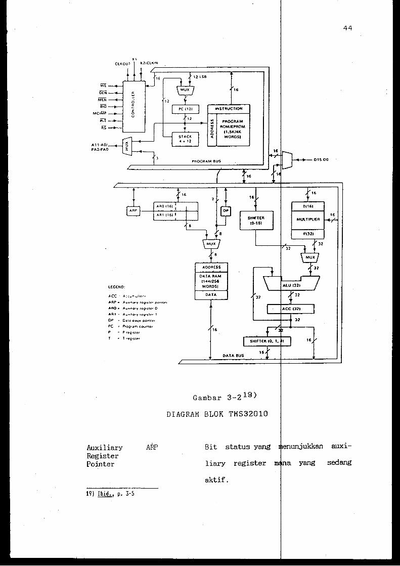
Diagram blok TMS32010 ditunjukkan a gambar 3-2.
Keterangan untuk tiap bagian pacta ar tersebut
adalah sebagai berikut:
SIMBOL
Accumulator ACC Accumulator terbagi menjadi
high-order word (b t 31-16) dan low-
order word (bit 15-0), digunakan
Arithmatic ALU Adalah unit bit Logic Unit 2's komplement, dua input
32 bit dan satu yang
d igunakan untuk accumulator.
Auxiliary ARO,AR1 Dua register Registers
untuk data addressing dan
Kesembilan bit
terbawah pada register dapat
digunakan untuk
WE
O£N
MiN 810
MCtM~
ii\1
iiS
A11·AO/ PA2·PA0
l£G£NO:
AAP • Au .. h..,v reg.stet co•nt~
ARO s Ay.,l•aty tCQtUCf 0
AR 1 4 Au .. lo.lllry tCQ•ih"t I
OP Oo~u I>A~e poontet
PC PrOQr am covnte'
p - p 'f!Q•~1Cf
T reg•ltf"f
Auxiliary ARP Register Pointer
19) Ibid., p. 3-5
OATA RAM (14412!>6
WORDS I
HS
Gambar 3-219)
DIAGRAM BLOK TMS32010
Bit status yang
liary register
aktif.
44
Hl-+-01!>00
16
"ukkan auxi-
yang sedang
Central Arithmatic Logic Unit
Data Bus
CALU
D(15-0)
Data Memory DP Page Pointer
Data RAM
External A(ll-0)/ Address Bus PA(2-0)
Interrupt INTF Flag
Interrupt INTM Mode
Multiplier MULT
Overflow ov Flag
Overflow OVM Mode
P Register p
Program Bus P(15-0)
45
Gabungan dari multiplier,
Bus digunakan untuk
j alur data dari
uk data page
menyim-
Bus 12 bit untuk
meng-address ekster-
nal. terendah adalah
address port I/0.
Flag menunjukkan
adanya interrupt
Bit status untuk interrupt
flag.
Parallel
bit.
Bit status flag yang menunjukkan
adanya overflow operasi arit-
matik.
Bit status yang menentukan mode
saturated a tau dalam
operasi aritmatik.
Register berisi hasil
kali dari
Bus 16 bit untuk
instruksi dari
Program Counter
Program ROM
Shifter
Stack
Status
T Register
PC(l1-0)
ST
T
III.3 ORGANISASI KEKORI
46
Register 12 bit digunakan untuk
meng-address program. PC
selalu berisi dari instruksi
dieksekusi. Isi
operasi pen-
decode-an inst
1,5K word on-chip ROM yang berisi
lwde program.
Ada dua shifter. barrel shifter
melakukan ri sebanyak 0
hingga 16 kali word memori data
yang diisikan ke ALU. Accumulator
parallel shifter melakukan geser
kiri sebanyak 0, 1 a tau 4 kali pada
seluruh isi dan menyim-
pan hasil
Hardware stack digunakan untuk
menyimpan terjadi
call.
berisi
bit-bit status
Register multi-
plicand selama i perkalian.
TMS32010 menggunakan arsitektur arvard dimana
memori data dan memori program terletak ada dua ruang
47
yang terpisah.
III.3.1 Memori Data
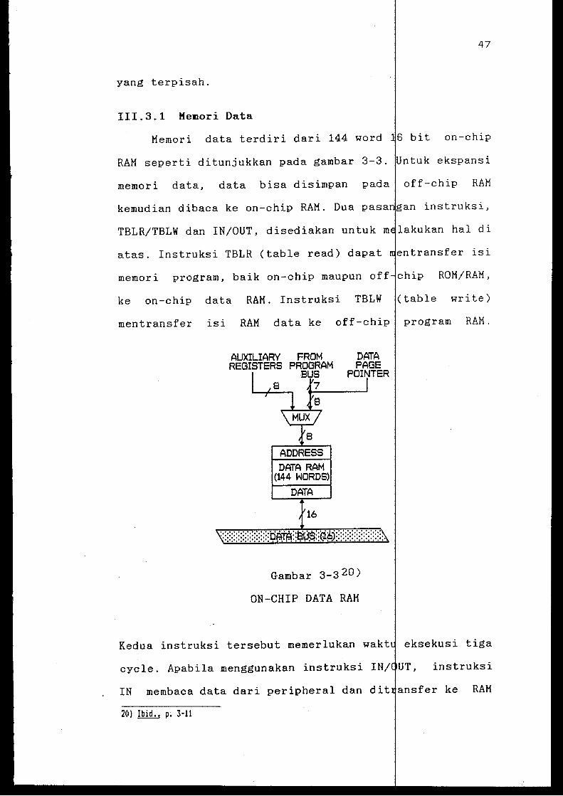
Memori data terdiri dari 144 word 1s bit on-chip
RAM seperti ditunjukkan pada gambar 3-3. ekspansi
memori data, data bisa disimpan off-chip RAM
kemudian dibaca ke on-chip RAM. Dua pas an instruksi,
TBLR/TBLW dan IN/OUT, disediakan untuk m lakukan hal di
I
atas. Instruksi TBLR (table read) dapat transfer isi
memori program, baik on-chip maupun off chip ROM/RAM,
ke on-chip data RAM. Instruksi TBLW (table write)
mentransfer isi RAM data ke off-chip program RAM.
AUXILIARY FROM REGISTERS PROGRAM
BUS 7
DATA RAM (144 WORDS)
DATA
16
DATA PAGE
POINTER
::::::::::::::::::::::oA~::@.::(i~):::::::::::::::::::::.
Gambar 3-3 20)
ON-CHIP DATA RAM
Kedua instruksi tersebut memerlukan wakt eksekusi tiga
cycle. Apabila menggunakan instruksi IN UT, instruksi
IN membaca data dari peripheral dan 'ansfer ke RAM
20) Ibid., p~ 3-11
48
data. Dengan menggunakan beberapa peran tambahan,
instruksi IN dan OUT dapat digunakan unt dan
menulis data dari RAM data ke peral penyimpan
eksternal yang sudah ditentukan alamatn ini
lebih cepat karena instruksi IN dan OUT ya memerlu-
kan waktu eksekusi dua cycle.
III.3.2 Memori Program
Progam memori terdiri dari l,5K wo pad a device.
On-chip program ROM memungkinkan program pada
kecepatan penuh tanpa memerlukan memori ekster-
nal kecepatan tinggi.
Operasi memori program dapat dipili dengan meng-
atur pin MC/MP (microcomputer/microprose pin
tersebut diset high berarti mode omputer. Se-
dangkan bila diset low berarti mode rosesor.
Dalam mode mikrokomputer hanya iakan lokasi
0 sampai 1523 dari ROM untuk pemakai. S lokasi
1524-1535 digunakan untuk keperluan peng esan. Memori
program sebanyak 2,5K dapat ditambahkan ada off-chip
ROM. Sedangkan dalam mode mikroprosesor luruh memori
program 4Kx16 bit ditempatkan pada ROM e
III.3.3 Perpindahan Data
TMS32010 menyediakan instruksi fungsi-fungsi
perpindahan data pada on-chip RAM. DMOV (data
move) berguna dalam implementasi algorit meng-
gunakan operasi delay z- 1 , seperti konvo usi dan filter I
digital.
49
Fungsi DMOV memungkinkan suatu isi lokasi
memori data yang sedang di-address dal on-chip RAM
disalin ke lokasi yang lebih tinggi, data
pada lokasi yang di-address pad a cycle
yang sama (misalnya pada instruksi U). Instruk-
Sl LTD (isi Register T, jumlahkan hasil kali
sebelumnya dan pindahkan data) juga me fungsi
DMOV.
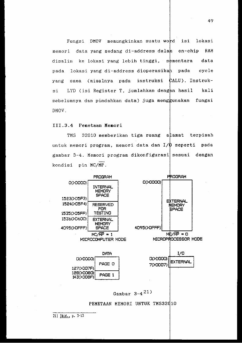
III.3.4 Penetaan Kemori
TMS 32010 memberikan tiga ruang a amat terpisah
untuk memori program, memori data dan I seperti pada
gambar 3-4. Memori program dikonfigurasi sesuai dengan
kondisi pin MC/MP.
0()0000)
1523(>05F3) 1524(>05F4)
1535()05FF) 1536()0600)
4095(>0FFF)
PROGRAM
INTERNAL MEMORY SPACE
RESERVED FOR
TESTING
EXTERNAL MEMORY SPACE
MC/MP = 1 MICROCOMPUTER MODE
DATA 0()0000)
PAGE 0 127(>007F) 1----~ 128()0080) 143(>008F) ....._P_A_G_E_l---J
0()0000)
Gambar 3-4 21 )
PEMETAAN MEMORI UNTUK TKS32 (0 21) Ibid., p. 3-13
50
III.3.5 Auxiliary Register
TMS32010 mempunyai dua auxiliary r gister 16 bit
(ARO dan AR1). Pada bagian ini akan d bahas masing-
masing mengenai fungsi register dan baga mana auxiliary
register ini dipilih, diisi dan disimpan isinya.
Auxiliary register dapat digunakan ntuk indirect
addressing dari memori data, penyimpan d ta semen tara
dan sebagai loop control. Indirect addre sing dilakukan
dengan meletakkan address memori data dari operand
suatu instruksi pada kedelapan bit tere dah auxiliary
register. Register dipilih dengan single bit Auxiliary
Register Pointer (ARP) yang diisi harga atau 1, yang
masing-masing menunjukkan ARO atau AR1. RP ini merupa
kan bagian dari register status dan dap t disimpan di
memori.
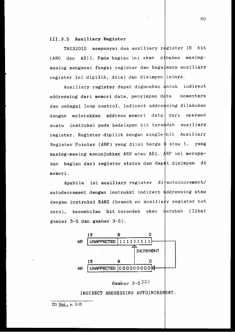
Apabila isi auxiliary register di autoincrement/
autodecrement dengan instruksi indirect
dengan instruksi BANZ (branch on auxilia
zero), kesembilan bit terendah akan
gambar 3-5 dan gambar 3-6).
lo AR UNAFFECTED
1-o
8
8
0
INCREMENT
0
ressing atau
register not
(lihat
AR UNAFFECTED 0 0 0 0 0 0 0 0 0 ~--ll---'
Gambar 3-5 22 )
INDIRECT ADDRESSING AUTOINCRE NT.
22) Ibid., p. 3-15
15 8 0
AR UNAFFECTED 1 1 1 1 1 1 1 1 1 IH---1----l
DECREMENT 15 0
AR
Gambar 3-6 23)
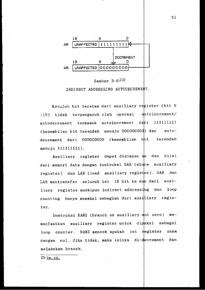
INDIRECT ADDRESSING AUTODECREM
Ketujuh bit teratas dari auxiliary r ister (bit 9
-15) tidak terpengaruh oleh operasi to increment/
autodecrement termasuk autoincrement 111111111
(kesembilan bit terendah menuju 00000000 auto-
decrement dari 000000000 (kesembilan terendah
menuju 111111111).
Auxiliary register dapat disimpan dan diisi
dari memori data dengan instruksi SAR (st auxiliary
register) dan LAR (load auxiliary regis dan
LAR mentransfer seluruh isi dari auxi-
liary register meskipun indirect address· dan loop
counting hanya memakai sebagian dari aux regis-
ter.
Instruksi BANZ (branch on auxiliary me-
manfaatkan auxiliary register untuk di ai sebagai
loop counter. BANZ mencek apakah isi sam a
dengan nol. Jika tidak, maka isinya di- crement dan
melakukan branch.
23) Loc. cit.
52
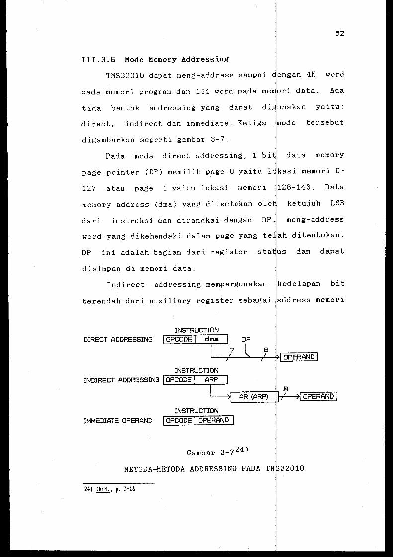
III.3.6 Kode Memory Addressing
TMS32010 dapat meng-address sampai engan 4K word
pada memori program dan 144 word pada me ri data. Ada
tiga bentuk addressing yang dapat di yaitu:
direct, indirect dan immediate. Ketiga ode tersebut
digambarkan seperti gambar 3-7.
Pada mode direct addressing, 1 bi data memory
page pointer (DP) memilih page 0 yaitu 1 kasi memori 0-
127 atau page 1 yaitu lokasi memori 128-143. Data
memory address (dma) yang ditentukan ole ketujuh LSB
dari instruksi dan dirangkai dengan DP, meng-address
word yang dikehendaki dalam page yang te ah ditentukan.
DP ini adalah bagian dari register sta s dan dapat
disimpan di memori data.
Indirect addressing mempergunakan kedelapan bit
terendah dari auxiliary register sebagai address memori
INSTRUCTION DIRECT ADDRESSING
INSTRUCTION
AR (ARP)
INSTRUCTION IMMEDIATE OPERAND I OPCODE I OPERAND I
Gambar 3-7 24 )
METODA-METODA ADDRESSING PADA TM 32010
24) Ibid., p. 3-lb
data yang cukup untuk meng-address 144 wo
memerlukan penentuan page. Auxiliary r
dengan auxiliary register pointer (
register dapat dibuat autoincrement/dec
suatu instruksi indirect addressing dibe
ment/decrement ini terjadi setelah
sedang berlangsung selesai dieksekusi.
Bila digunakan mode immediate, oper
ke dalam word instruksi itu sendiri.
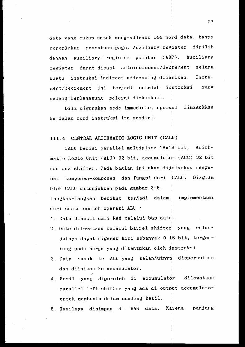
III.4 CENTRAL ARITHMATIC LOGIC UNIT (
CALU berisi parallel multiplier
matic Logic Unit (ALU) 32
dan dua shifter. Pada bagian ini akan dij
nai komponen-komponen dan fungsi dari
blok CALU ditunjukkan pada gambar 3-8.
Langkah-langkah berikut terjadi dalam
dari suatu contoh operasi ALU :
1. Data diambil dari RAM melalui
2. Data dilewatkan melalui barrel shifte
data, tanpa
dipilih
Auxiliary
selama
Incre
yang
dimasukkan
bit, Arith
(ACC) 32 bit
menge
U. Diagram
implementasi
yang selan-
jutnya dapat digeser kiri sebanyak 0- bit, tergan
tung pada harga yang ditentukan oleh struksi.
3. Data masuk ke ALU yang selanjutn dioperasikan
dan diisikan ke accumulator.
4. Hasil yang diperoleh di accumulat
parallel left-shifter yang ada di ou
untuk membantu dalam scaling hasil.
5. Hasilnya disimpan di RAM data.
dilewatkan
t accumulator
en a panjang
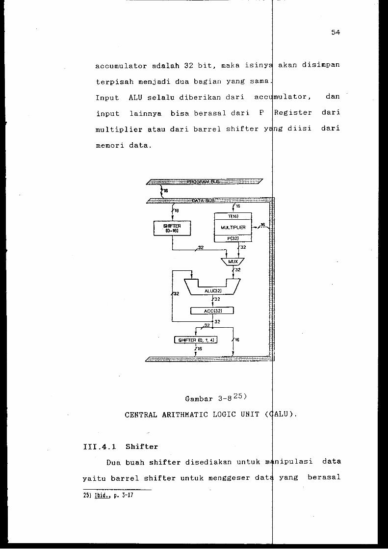
54
accumulator adalah 32 bit, maka isiny akan disimpan
terpisah menjadi dua bagian yang
Input ALU selalu diberikan dari
input lainnya bisa berasal dari P
multiplier atau dari barrel shifter
memori data.
Gambar 3-8 25 )
CENTRAL ARITHMATIC LOGIC UNIT ( ALU).
III.4.1 Shifter
dan
dari
dari
Dua buah shifter disediakan untuk 1
nipulasi data
yaitu barrel shifter untuk menggeser dat yang berasal
25) Ibid., p. 3-17
55
dari RAH data untuk diisikan ke ALU, dan parallel
shifter untuk menggeser isi accumula or yang akan
disimpan ke RAH data (lihat gambar 3-8).
Barrel shifter memiliki input 16 b t yang terhu-
bung ke bus data dan output 32 bit yang terhubung ke
ALU. Barrel shifter melakukan geser ki sebanyak 0
hingga 16 bit pada seluruh word memori d yang dima-
sukkan ke dalamnya, dikurangkan ditambahkan
ke accumulator dengan instruksi LAC, dan ADD.
Dengan arithmatic left-shift, shifter me harga nol
pada LSB dan memberi tanda perluasan pad word memori
data 16 bit menjadi 32 bit (misalnya b t di sebelah
kiri HSB pada word data diisi 1 bila isi HSB sebelumnya
berharga 1 atau diisi 0 bila HSB sebelu Hal ini
berbeda dengan logical left-shift yang mengisi
harga 0 di sebelah kiri HSB.
Parallel shifter hanya dapat dengan
instruksi SACH (store high-order ac lator word).
Instruksi ini mengakibatkan shifter di dengan 32
bit isi akumulator, kemudian r ke kiri. Ke
16 bit HSB pada shifter disimpan di RAH, sehingga meng-
akibatkan hilangnya bit-bit high-order. Sedangkan Isi
accumulator tetap tidak berubah. Paralle shifter hanya
dapat melakukan pergeseran sebanyak 0, atau 4. Per-/
geseran 1 dan 4 digunakan untuk operas -operasi per-
kalian. Pergeseran ke kanan secara lang ng tidak dapat
dilakukan di sini.
56
111.4.2 ALU dan Accumulator
ALU dan Akumulator 32 bit seper i gambar 3-8
melaksanakan fungsi-fungsi aritmatik d logika dalam
jangkauan yang luas, yang mayoritas d lakukan dalam
satu clock cycle. Setiap kali suatu oper si dikerjakan
di ALU, hasilnya ditransfer ke accumul tor yang se-
lanjutnya dapat dilakukan operasi la nnya seperti
pergeseran. Data yang masuk ke ALU bisa diambil dari
barrel shifter.
ALU adalah suatu unit logika a itmatik yang I
bekerja pada word data 16 bit, dan hasil loperasinya 32
bit. ALU dapat menambah, mengurangi dan melakukan
operasi-operasi logika. Accumulator se alu merupakan
destinasi dan operand utama. Hasil erasi logika
seperti pada tabel 3-1. Harga memori d (dma) adalah
operand untuk setengah bagian bawah accumulator
(bit 15-0). Nol adalah operand untuk bag ian
atas isi accumulator.
Tabel 3-1. HASIL-HASIL OPERASI LOGIKA MULATOR 26 )
Fungsi Ace bit 31-16 Ace
XOR (O).XOR.(ACC (31-16))
AND (O).AND.(ACC (31-16))
OR (O).OR.(ACC (31-16))
.(ACC (15-0))
(dma).AN .(ACC (15-0)) I
(dma).OR (ACC (15-0))
Accumulator 32 bit menyimpan out t dari ALU,
yang juga sering merupakan input kemba i untuk ALU.
Accumulator dibagi dalam dua word 16 bit ,untuk penyim-
2b) Ibid., p. 3-20 I
57
panan ke memori data yaitu high-order wo d (bit 31-16)
dan low-order word (bit 15-0). Untuk mel penyim-
panan high-order word dan low-order word
tor ke memori data digunakan instruksi S
Instruksi-instruksi ini dapat digunakan
tasi double-precision arithmetic.
Accumulator juga mampu mensimulasi
accumula-
H dan SACL.
alam implemen-
efek satu-
rasi dari sistem analog. Hal ini dapat d lakukan dengan
menggunakan mode saturasi accumulator, ng dikontrol
dengan bit register status OVM mode). Mode
saturasi accumulator di-enable atau di- dengan
menset atau mereset bit OVM melalui inst uksi SOVM dan
ROVM. Jika OVM diset dan operasi accumul tor menghasil
kan overflow, maka accumulator langan paling
positif atau paling negatif, tergantu pada tanda
dari operand dan hasil accumulator
pada keadaan saturasi adalah 7FFFFFFF positif) atau
80000000 (negatif). Jika OVM direset dan terjadi over-
flow, hasil overflow dimasukkan ke
modifikasi. Sedangkan dalam operasi lo
menghasilkan overflow.
Pengaktifan mode saturasi diperluk
isi accumulator merupakan representas
sinyal, karena bila mode satuasi I
overflow mengakibatkan diskontinyuitas y
harapkan dalam representasi bentuk g
tanpa
dapat
terutama bila
harga suatu
diaktifkan,
g tidak di
Dalam
keadaan mode saturasi, perilaku akumulat r sangat mirip
dengan keadaan sistem analog yang
maksimum atau saturasi bila. diberi
lu besar.
Apabila terjadi overflow, bit OV (
register status diset, tidak perduli ap
diset atau tidak. Instruksi BV (branch
yang melakukan branch hanya bila OV dise ,
kan program membuat keputusan berdasar
kah telah terjadi overflow atau tidak.
maka OV hanya dapat direset dengan inst
dengan mengisi langsung register
adalah bagian dari register status
dapat disimpan dalam memori data dengan
(store status register) atau dapat
struksi LST (load status register).
TMS32010 ini juga dapat melakukan
yang bergantung pada status ALU
Instruksi-instruksi seperti BLZ, BLEZ,
BZ akan mengakibatkan terjadinya branc
kondisi tertentu.
III.4.3 Multiplier, T Register dan P
58
capai batas
1 yang terla-
erflow) pada
ah bit OVM
n overflow),
memungkin-
kondisi apa
la OV diset,
ksi BV atau
Karena OV
kondisinya
SST
dengan in-
truksi branch
akumulator.
BNZ,
menemui
TMS32010 menyediakan hardware 16x16
bit yang mampu melakukan operasi perkal· dalam satu
machine cycle .dengan hasil kali 32 bit. register
berikut mempunyai kaitan erat dengan plier, yaitu:
Temporary Register (T) 16 bit yang operand-
operand untuk multiplier.
Product Register (P) 16 bit yang
kali.
Untuk menggunakan multiplier
harus diisikan ke T register
59
hasil
-mula operand
data dengan
instruksi LT, LTA atau LTD. Kemudian instruksi MPY
(multiply) atau MPYK (multiply
operand kedua yang juga melalui
gunakan instruksi MPY, maka harga penga
langan 16 bit. Sedangkan jika mengguna
pengali adalah konstanta immediate 13 bi
memberikan
Jika meng
adalah bi
MPYK, harga
yang berada
dalam word instruksi MPYK. Setelah ekse si selesai,
tersebut hasil kali ditempatkan di P register.
selanjutnya dapat ditambahkan, dikur an atau diisi
kan ke akumulator dengan instruksi PAC, AC, SPAC, LTA
atau LTD.
Isi P register tidak dapat diubah mengubah
register-regiser yang lain. Terjadinya
dilayani hingga instruksi yang
MPY/MPYK selesai dieksekusi. Oleh
si perkalian hendaknya selalu
yang menghubungkan P register
III.5 SISTEK KONTROL
tidak
instruksi
itu instruk
instruksi
Sistem kontrol pada TMS32010 dila kan oleh pro-
gram counter dan stack, sinyal
rupt dan register status.
ernal, inter-
60
III.5.1 Program Counter dan Stack
Program counter dan stack digunakan ntuk eksekusi
instruksi-instruksi branch, interrupt
dan table read/table write. Program r (PC) adalah
register 12 bit yang berisi address program dari
instruksi berikutnya yang akan
membaca instruksi dari lokasi memori pr
address oleh PC dan isi PC secara
TMS32010
am yang di
increment
menyiapkan instruksi berikutnya diambil. PC
diinisialisasi ke harga 0 dengan mengakt kan pin reset
( RS).
Seperti dikemukakan sebelumnya
menggunakan arsitektur Harvard yang dim
arsitektur Harvard ruang memori program
terpisah, sehingga memungkinkan
instruksi dan eksekusi dilakukan secara
3-9 memperlihatkan hal ini.
Memori program selalu di-address
PC dapat diubah oleh instruksi
branch yang diuji adalah benar.
langsung increment ke address instru
Semua branch di sini adalah absolut, ti
relative, jadi harga 12 bit yang did
instruksi branch diisi langsung ke PC
TMS32010
Pad a
memori data
pengambilan
erlap. Gambar
PC. Isi
kondisi
maka PC
berikutnya.
ada branch
dari word
r melakukan
branch. Bila terjadi interrupt atau ins ksi subrou
tine call, isi PC di-push ke stack untuk enjaga kemba
linya hubungan dengan konteks program se lumnya.
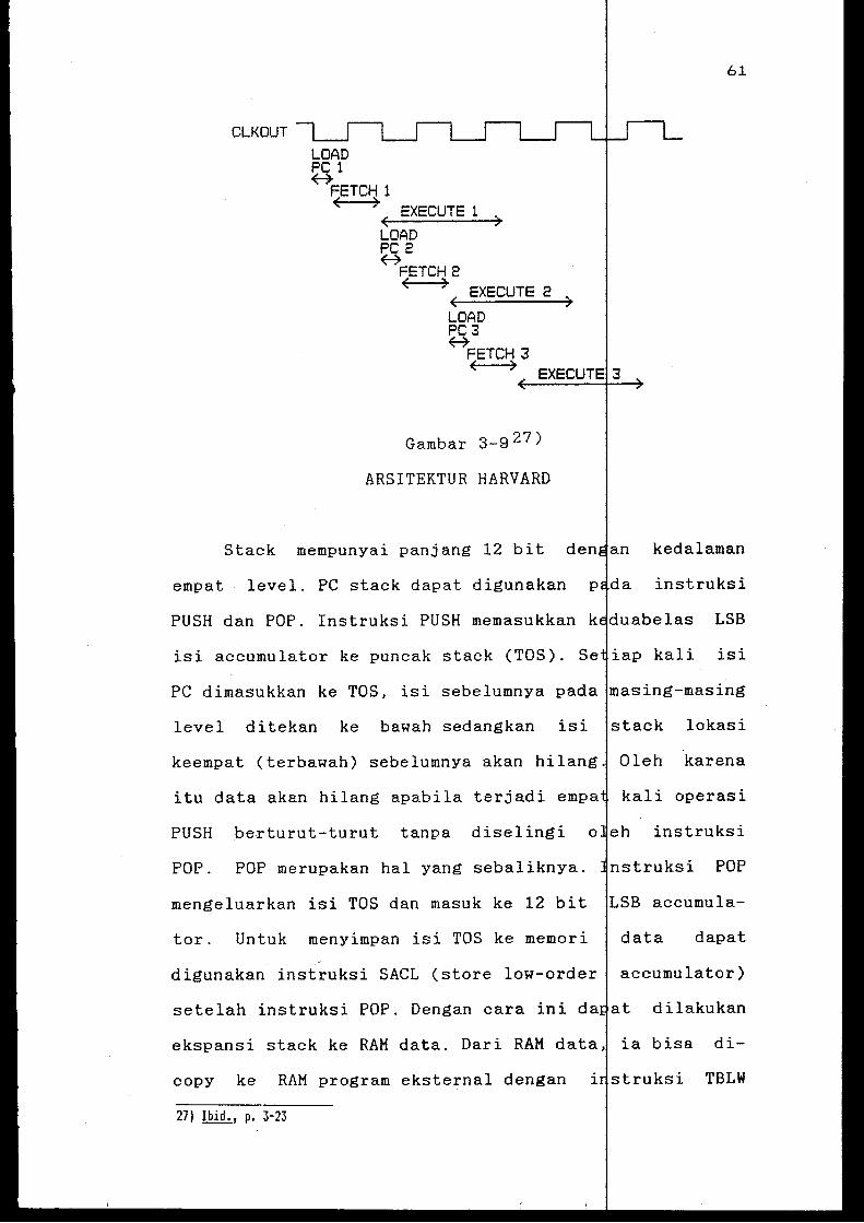
CLKOUT LOAD PC 1 ~
FETCH 1 ( )
( EXECUTE 1 )
LOAD PC 2 ~
FETCH 2 < ) < EXECUTE 2 )
LOAD PC3 ~
FETCH 3 ( )
Gambar 3-9 27 )
ARSITEKTUR HARVARD
Stack mempunyai panjang 12 bit den
61
3
kedalaman
empat level. PC stack dapat digunakan p a instruksi
isi accumulator ke puncak stack (TOS). Se iap kali isi
PC dimasukkan ke TOS, isi sebelumnya pada masing-masing
level ditekan ke bawah sedangkan isi stack lokasi
keempat (terbawah) sebelumnya akan hilang Oleh karena
itu data akan hilang apabila terjadi empa kali operasi
PUSH berturut-turut tanpa diselingi o eh instruksi
POP. POP merupakan hal yang sebaliknya. nstruksi POP
mengeluarkan isi TOS dan masuk ke 12 bit LSB accumula-
tor. Untuk menyimpan isi TOS ke memori data dapat
digunakan instruksi SACL (store low-order accumulator)
setelah instruksi POP. Dengan cara ini d 1
at dilakukan I
ekspansi stack ke RAM data. Dari RAM data ia bisa di-
copy ke RAM program eksternal dengan TBLW
27) Ibid., p. 3-23
62
(table write). Dengan cara ini stack d 1 at diekspansi
ke level yang sangat besar.
III.5.2 Reset
Reset (RS) adalah non-maskable exte nal interrupt
yang dapat digunakan setiap saat. Reset secara normal
diberikan setelah supply dinyalakan pada saat prosesor
dalam keadaan tidak tentu (acak). Input eset low harus
diberikan sedikitnya lima clock cycle.
Pada saat menerima sinyal RS, akan
berikut:
1. DEN, WE, dan MEN menuju high.
2. Bus data D15-DO berada pada keadaan
3. PC berisi 0 dan All-AO juga berisi
cycle berikutnya setelah RS menuju lo
4. Interrupt di-disable dan interrupt
seluruhnya direset.
erjadi proses
h impedance.
pada clock
flag register
TMS32010 dapat direset selama waktu yang tak terbatas.
Bit-bit status ARP, DP dan OVH tidak diinisialisasi
oleh reset. Jadi ini bit-bit ini henda nya bisa di
inisialisasi dengan software setelah res t.
III.5.3 Register Status
Register status terdiri dari lima b t status. Bit
bit status ini dapat diubah secara endiri-sendiri
dengan instruksi yang sesuai. itu instruksi
SST melayani penyimpanan register us ke memori
data. Instruksi LST mengisi register st us dari memori
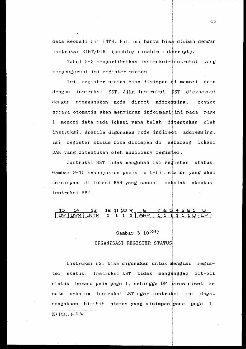
6 7 0
data kecuali bit INTM. Bit ini hanya bis diubah dengan
instruksi EINT/DINT (enable/ disable
Tabel 3-2 memperlihatkan instruksi- struksi yang
mempengaruhi isi register status.
Isi register status bisa disimpan memori data
dengan instruksi SST. Jika instruksi dieksekusi
dengan menggunakan mode direct addre device
secara otomatis akan menyimpan informasi ini pada page
1 memori data pada lokasi yang telah d tentukan oleh
instruksi. Apabila digunakan mode indire t addressing,
isi register status bisa disimpan di s lokasi
RAM yang ditentukan oleh auxiliary regis er.
Instruksi SST tidak mengubah isi re ister status.
Gambar 3-10 menunjukkan posisi bit-bit s atus yang akan
tersimpan di lokasi RAM yang sesuai se eksekusi
instruksi SST.
Gambar 3-1028)
ORGANISASI REGISTER STATUS
Instruksi LST bisa digunakan untuk regis-
ter status. Instruksi LST tidak ap bit-bit
status berada pada page 1, sehingga DP ke
satu sebelum instruksi LST agar instru ini dapat
mengakses bit-bit status yang disimpan page 1.
28) Ibid., p. 3-2b
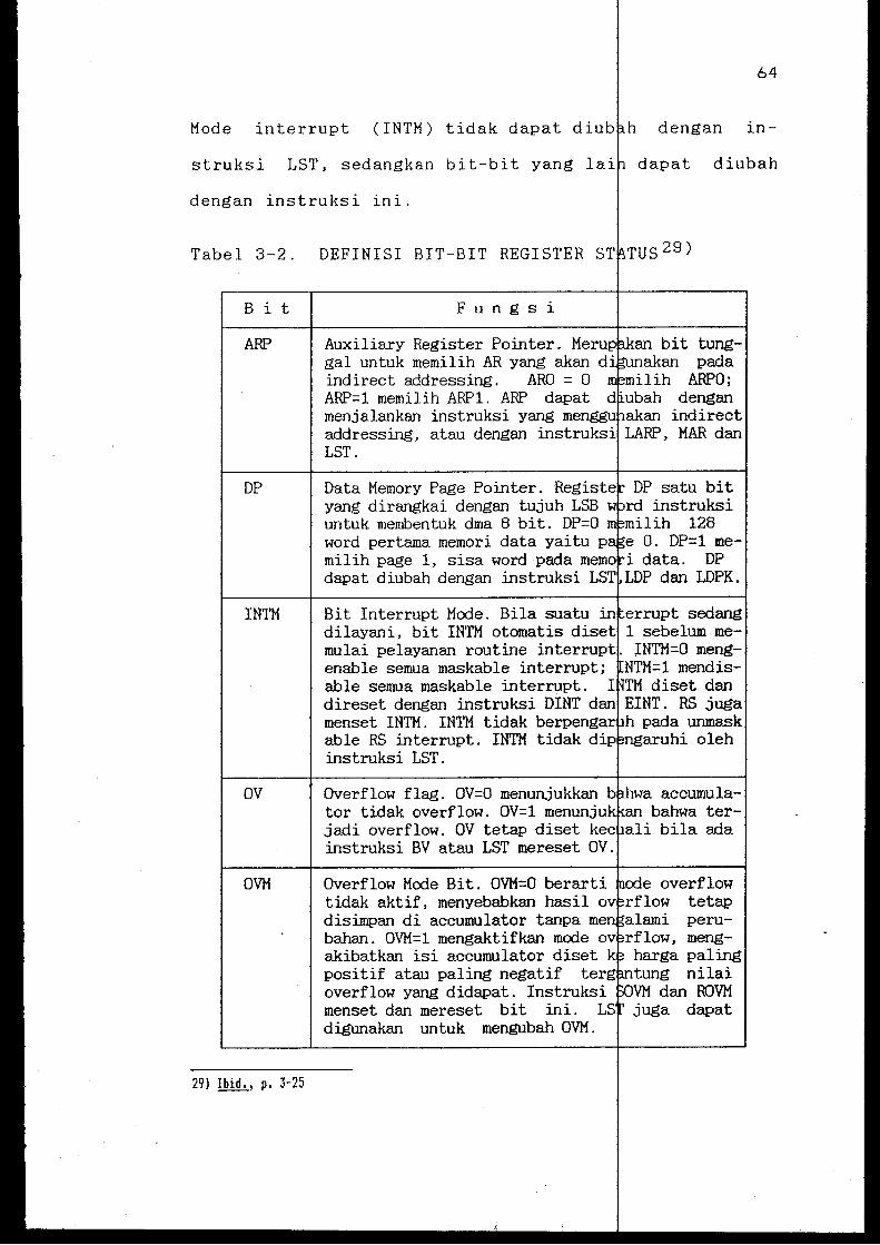
64
Mode interrupt (INTM) tidak dapat diub. h dengan in-
struksi LST, sedangkan bit-bit yang lai dapat diubah
dengan instruksi ini.
Tabel 3-2. DEFINISI BIT-BIT REGISTER ST TUs29)
B i t F u n g s i
ARP Auxiliary Register Pointer. gal untuk memilih AR yang akan d indirect addressing. ARO = 0 ARP=1 memilih ARP1. ARP dapat menjalankan instruksi yang addressing, atau dengan instruks LST.
DP Data Memory Page Pointer. Regis
INTM
ov
OVM
29) Ibid., p. 3-25
yang dirangkai dengan tujuh LSB untuk membentuk dma 8 bit. DP=O lUI='lll.L.L word pertama memori data yaitu milih page 1, sisa word pada dapat diubah dengan instruksi
Bit Interrupt Mode. Bila suatu dilayani, bit INTM otomatis mulai pelayanan routine ~.._~_.-.
enable semua maskable interrupt; able semua maskable interrupt. direset dengan instruksi DINT menset INTM. INTM tidak ho·..-.... ,,.n .. r<:>
able RS interrupt. INTM tidak d instruksi LST.
sedang 1 sebelum me
JNTM=O mengNTM=1 mendis-
diset dan EINT. RS juga
pada unmask hi oleh
Overflow flag. OV=O menunjukkan accumula-tor tidak overflow. OV=1 menunju bahwa ter-j ad i overflow. OV tetap d iset K~•~..:uz1.1 i b i la ada instruksi BV atau LST mereset OV.
Overflow Mode Bit. OVM=O berarti tidak aktif, menyebabkan hasil disimpan di accumulator tanpa bahan. OVM=1 mengaktifkan mode akibatkan isi accumulator diset positif atau paling negatif overflow yang didapat. Instruksi menset dan mereset bit 1n1. digunakan untuk mengubah OVM.
!I;,Cl.LaJui perulow, meng
harga paling tung nilai
dan ROVM juga dapat
III.6 FUNGSI INPUT/OUTPUT
TMS 32010 melakukan bermacam-mac
untuk berhubungan dengan peralatan
paralel 16 bit dapat dimanfaatkan
65
fungsi I/0
Bus data
melakukan
fungsi-fungsi I/0 dalam dua clock cycle engan instruk-
si IN dan OUT. Port-port I/0 diberi addr ketiga
LSB bus address (PA2-PAO). Pengambil input untuk
operasi-operasi tes bit dan branch dan input
interrupt (INT) diberikan untuk memberik fleksibeli-
tas pada sistem.
Desain I/0 disederhanakan dengan
sama seperti memori. Peralatan I/0 dipe
ruang address I/0 menggunakan address
sor dan bus-bus data yang sama dengan
Input/output data dari dan ke
dilakukan dengan instruksi IN dan OUT.
melalui bus data 16 bit ke dan dari memo
mengaktifkan dua strobe yang
enable (DEN) dan write enable (WE).
erlakukan I/0
dalam
prose-
eralatan luar
ditransfer
data dengan
yaitu data
Bus data eksternal dua arah selalu dalam kondisi
high impedance kecuali bila WE aktif low WE menuju low
selama cycle pertama instruksi OUT dan selama cycle
kedua instruksi TBLW.
III.6.1 Operasi Input/Output
Ketiga pin port address (PA2-PAO mengeluarkan
address port selama instruksi OUT. Ekse usi instruksi
IN membangkitkan strobe DEN untuk mentr sfer data dari
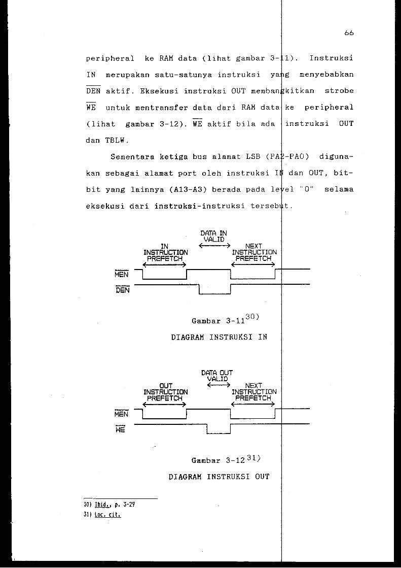
66
peripheral ke RAM data (lihat gambar 3- 1). Instruksi
IN merupakan satu-satunya instruksi y g menyebabkan
DEN aktif. Eksekusi instruksi OUT memban kitkan strobe
WE untuk mentransfer data dari RAM data ke peripheral
(lihat gambar 3-12). WE aktif bila ada instruksi OUT
dan TBLW.
Sementara ketiga bus alamat LSB CPA -PAO) diguna-
kan sebagai alamat port oleh instruksi I dan OUT, bit-
bit yang lainnya (A13-A3) berada pada 1 el "0" selama
eksekusi dari instruksi-instruksi terse t.
MEN
DEN
MEN
WE
30) Ibid., p. 3-29 31) loc. cit.
DATA IN VALID
IN ( ) NEXT INSTRUCTION INSTRUCTION PREFETCH PREFETCH
( )~------~( )~-----
30) Gambar 3-11
DIAGRAM INSTRUKSI IN
DATA OUT VALID
OUT ( ) NEXT INSTRUCTION INSTRUCTION PREFETCH PREFETCH
E > ________ ~E )~-----
Gambar 3-12 31)
DIAGRAM INSTRUKSI OUT
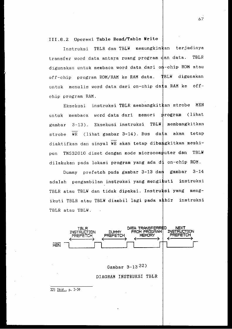
67
III.6.2 Operasi Table Read/Table Write
Instruksi TBLR dan TBLW memungkin an terjadinya
transfer word data anta~a ruang program an data. TBLR
digunakan untuk membaca word data dari o -chip ROM atau
off-chip program ROM/RAM ke RAM data. BLW digunakan
untuk menulis word data dari on-chip da a RAM ke off-
chip program RAM.
Eksekusi instruksi TBLR membangkit an strobe MEN
untuk membaca word data dari memori rogram (lihat
gambar 3-13). Eksekusi instruksi TBLW membangkitkan
strobe WE (lihat gambar 3-14). Bus da a akan tetap
diaktifkan dan sinyal WE akan tetap dib meski-
pun TMS32010 diset dengan mode microcom ter dan TBLW
dilakukan pada lokasi program yang ada d on-chip ROM.
Dummy prefetch pada gambar 3-13 d gambar 3-14
adalah pengambilan instruksi yang mengi ti instruksi
TBLR atau TBLW dan tidak dipakai.
ikuti TBLR atau TBLW diambil lagi pada
TBLR atau TBLW.
MEN
TBLR INSTRUCTION PRE FETCH
( )
32) Ibid., p. 3-30
DUMMY PREFETCH
( )
Gambar 3-13 32)
DIAGRAM INSTRUKSI TBLR
meng-
instruksi
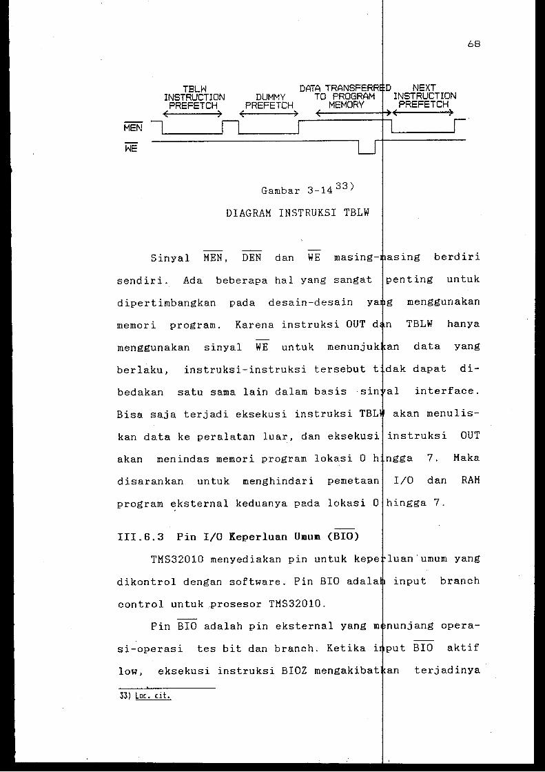
MEN
WE
TBLW INSTRUCTION
PREFETCH ( )
Gambar 3-14 33 )
DIAGRAM INSTRUKSI TBLW
Sinyal MEN, DEN dan WE masing-
sendiri. Ada beberapa hal yang sangat
dipertimbangkan pada desain-desain y
memori program. Karena instruksi OUT d
menggunakan sinyal WE untuk menunju
68
berdiri
untuk
menggunakan
TBLW hanya
data yang
berlaku, instruksi-instruksi tersebut t ak dapat di-
bedakan satu sama lain dalam interface.
Bisa saja terjadi eksekusi instruksi TBL akan menulis-
kan data ke peralatan luar, dan eksekusi instruksi OUT
akan menindas memori program lokasi 0 h ngga 7. Maka
disarankan untuk menghindari pemetaan I/0 dan I
program eksternal keduanya pada lokasi 0 lhingga 7.
III.6.3 Pin I/0 Keperluan Umum (BIO) I
RAM
TMS32010 menyediakan pin untuk kepe luan·umum yang
dikontrol dengan software. Pin BIO adala input branch
control untuk~prosesor TMS32010.
Pin BIO adalah pin eksternal yang unjang opera-
si-operasi tes bit dan branch. Ketika BIO aktif
low, eksekusi instruksi BIOZ mengakibat an terjadinya
33) loc. cit.
69
branch. Pin BIO ini berguna untuk emantau status
peralatan luar. Ini khususnya digunakan sebagai alter-
natif penggunaan interrupt bila loop ang memerlukan
waktu kritis (time-critical loop) tidak dapat diganggu.
Untuk sistem yang menggunakan inp t tak sinkron
dengan pin BIO pada TMS32010 (NMOS), di erlukan perang
kat eksternal untuk memastikan bahwa instruksi BIOZ
dieksekusi dengan semestinya. Perangkat ini mensinkron
kan sinyal input BIO dengan rising ed e dari CLKOUT
TMS32010.
III.7 INTERRUPT
TMS32010 menyediakan input. inte eksternal
untuk komunikasi dengan operasi-ope eksternal
yang kritis terhadap waktu. Interrupt d at dibangkit-
kan dengan memberikan sinyal negative- edge atau
suatu sinyal level low. pada pin input i terrupt. Inter
rupt pada TMS32010 dapat di-mask (m kable) dengan
menggunakan register status interrupt mode bit dan
beberapa bit mask.
Untuk sistem yang menggunakan inp tak sinkron
pada pin interrupt (INT) TMS32010, dipe lukan perangkat
luar untuk memastikan proses interrupt ekerja dengan
semestinya. Perangkat ini mensinkronka sinyal input
INT dengan rising edge CLKOUT dari TMS3 10.
Bila interrupt di-enable, interrup menjadi aktif
saat level low pada pin INT atau bil negative-edge
telah di-latch ke interrupt. flag ( INTF) . 1 Jika register
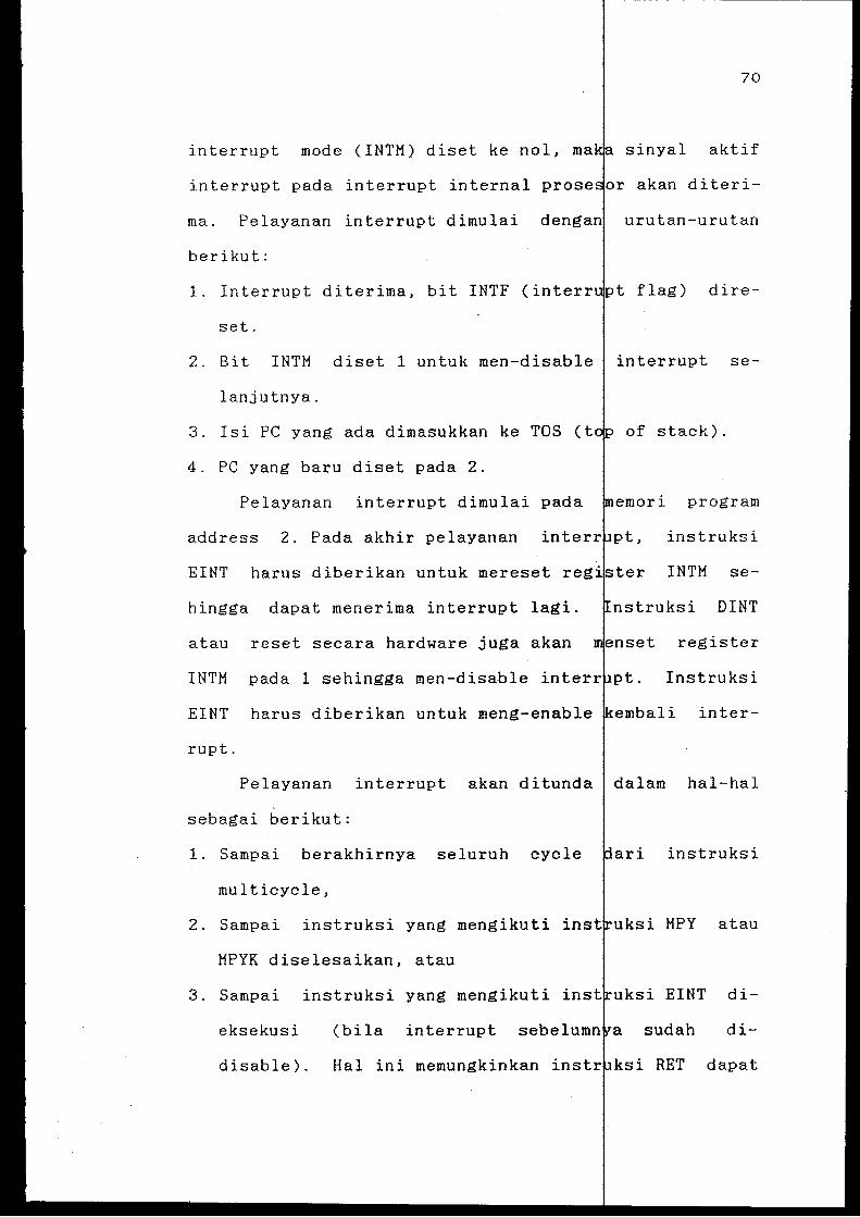
interrupt mode (INTM) diset ke nol, ma
interrupt pada interrupt internal
ma. Pelayanan interrupt dimulai den
berikut:
1. Interrupt diterima, bit INTF
set.
70
sinyal aktif
r akan diteri
urutan-urutan
t flag) dire-
2. Bit INTM diset 1 untuk men-disable interrupt se-
lanjutnya.
3. Isi PC yang ada dimasukkan ke TOS (t
4. PC yang baru diset pada 2.
Pelayanan interrupt dimulai pada
address 2. Pada akhir pelayanan inter
EINT harus diberikan untuk mereset reg·
hingga dapat menerima interrupt lagi.
atau reset secara hardware juga akan
INTM pada 1 sehingga men-disable inter
EINT harus diberikan untuk meng-enable
rupt.
of stack).
ri program
instruksi
INTM se
DINT
register
Instruksi
inter-
Pelayanan interrupt akan ditunda dalam hal-hal
sebagai berikut:
1. Sampai berakhirnya seluruh cycle
multicycle,
2. Sampai instruksi yang mengikuti ins
MPYK diselesaikan, atau
instruksi
ksi MPY atau
3. Sampai instruksi yang mengikuti ins uksi EINT di-
eksekusi (bila interrupt sudah di-
disable). Hal ini memungkinkan inst dapat
71
dieksekusi setelah interrupt di-enab e pada akhir
routine suatu interrupt.
Gambar 3-15 menunjukkan urutan 1
nstruksi yang
terjadi saat interrupt aktif. Dummy fet adalah in-
struksi yang diambil tetapi tidak diekse usi. Instruksi
ini akan diambil ulang dan dieksekusi s
interrupt selesai dilaksanakan.
FETCH DUMMY FETCH INSTRUCTION N INSTRUCTION
N+l
FETCH INSTRUCTION
DOe
routine
EXECUTE N DUMMY CYCLE EXECUTE 002
Gambar 3-15 34)
DIAGRAM WAKTU INTERRUPT
III.8 INSTRUKSI BAHASA ASSEMBLY TKS3201
TMS32010 memberikan set yang sangat
menunjang dalam aplikasi pemrosesan siny dan aplikasi
yang lain seperti kontrol dengan kecepat tinggi. Set
instruksi yang ditunjukkan pada 3.3 umumnya
terdiri dari satu cycle dan panjang satu
word, sehingga memungkinkan mengekse i instruksi
dengan kecepatan maksimum 6,25 MIPS. P a tabel 3.4
tampak bahwa hanya instruksi-instruksi anch dan l/0
yang memerlukan multicycle. Pada bagian 1
ini akan di-
34) Ibid., p. 3-34
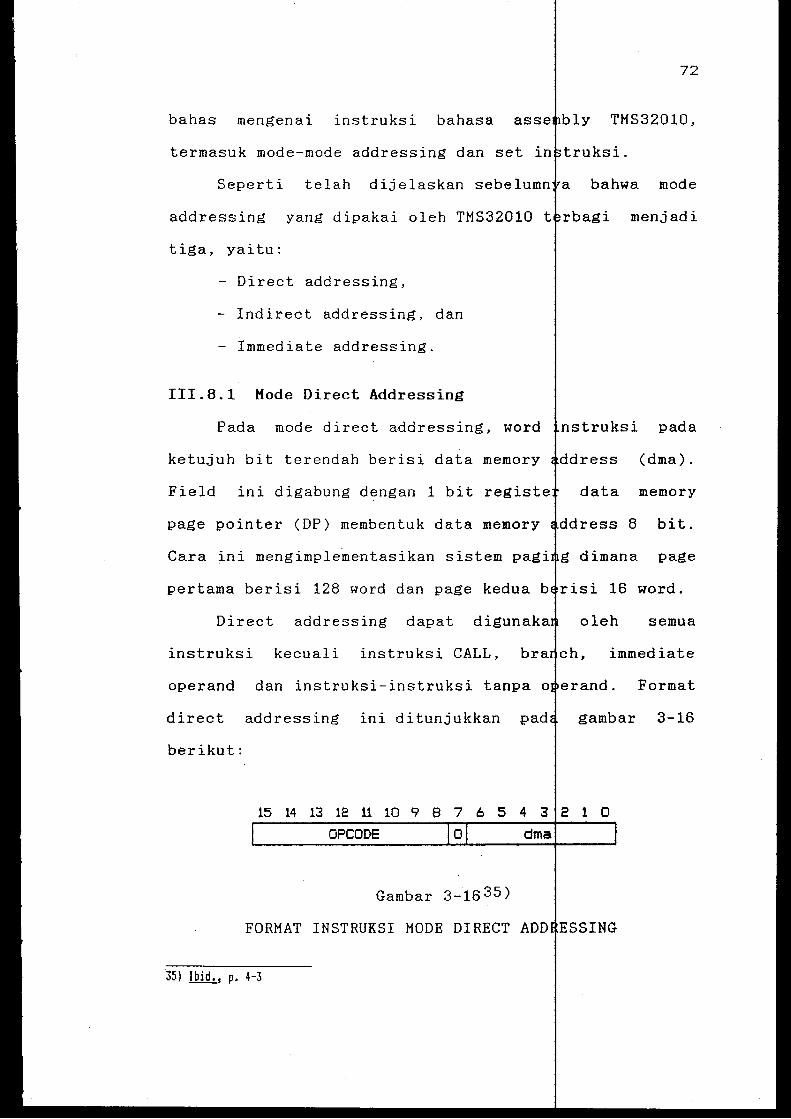
72
bahas mengenai instruksi bahasa ass ly TMS32010,
termasuk mode-mode addressing dan set in truksi. I
Seperti telah dijelaskan sebelumn a bahwa mode
addressing yang dipakai oleh TMS32010 t menjadi
tiga, yaitu:
- Direct addressing,
- Indirect addressing, dan
- Immediate addressing.
III.8.1 Mode Direct Addressing
Pada mode direct addressing, word pad a
ketujuh bit terendah berisi data memory (dma).
Field ini digabung dengan 1 bit data memory
page pointer (DP) membentuk data memory ress 8 bit.
Cara ini mengimplementasikan sistem pag dimana page
pertama berisi 128 word dan page kedua b word.
Direct addressing dapat digunak oleh semua
instruksi kecuali instruksi CALL, br immediate
operand dan instruksi-instruksi tanpa o Format
direct addressing ini ditunjukkan gambar 3-16
berikut:
15 14 13 12 11 10 9 8 7 6 5 4 3 2 1 0
OPCODE dma.
Gambar 3-1635)
FORMAT INSTRUKSI MODE DIRECT ADD ESSING
35} Ibid., p. 4-3
73
Bit 15 hingga 8 berisi opcode. bi 7 = 0 yang
menunjukkan mode addressing adalah direc
0 berisi data memory address (dma) yan
Bit 6 hingga
dapat meng-
address sampai dengan 128 word (1 page) memori data.
Untuk meng-address semua ruang memori d
data memory page pointer.
111.8.2 Mode Indirect Addressing
diperlukan
Indirect addressing membentuk data emory address
dari kedelapan bit terendah pada salah s tu dari auxi
liary register ARO dan AR1. Dengan indir ct addressing
ini cukup untuk mengaddress semua ru
tanpa memerlukan penentuan page.
Pointer (ARP) memilih auxiliary
dipakai. Auxiliary register dapat
increment atau di-decrement secara
kusi semua instruksi indirect,
tabel data dapat dilakukan dalam satu
decrement terjadi setelah instruksi
langsung selesai dieksekusi.
Berikut ini adalah simbol-simbol
dalam mode indirect addressing:
* lsi AR (ARP) digunakan sebagai dat•
* lsi AR (ARP) digunakan sebagai add
decrement Betelah mengakses memori d
*+ lsi AR (ARP) digunakan sebagai add
increment setelah mengakases memori
Format indirect addressing sepeerti pad a
memori data
iary Register
yang akan
otomatis di-
1 dengan ekse
manipulasi
le. Increment/
sedang ber-
ang digunakan
emory address.
ess, kemudian
ta.
ess, kemudian
ata.
gambar 3-17.
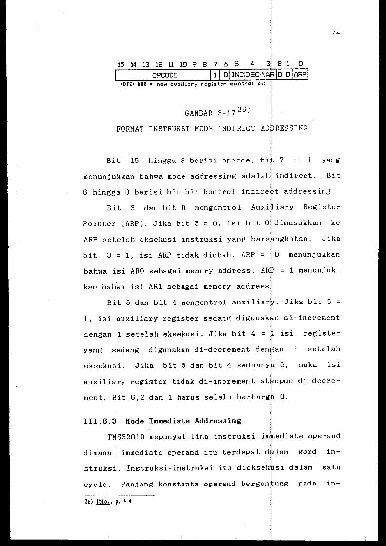
OPCODE NDTEI NRR = new ouxiliol'y l'egistel' conti'01 bit
GAMBAR 3-17 36 )
FORMAT INSTRUKSI MODE INDIRECT
74
SSING
Bit 15 hingga 8 berisi opcode, bi 7 = 1 yang
menunjukkan bahwa mode addressing
6 hingga 0 berisi bit-bit kontrol
Bit 3 dan bit 0 mengontrol
Pointer (ARP). Jika bit 3 = 0, isi
ARP setelah eksekusi instruksi yang bers
bit 3 = 1, isi ARP tidak diubah. ARP = bahwa isi ARO sebagai memory address. A
kan bahwa isi AR1 sebagai memory address
Bit 5 dan bit 4 mengontrol auxiliar
1, isi auxiliary register sedang diguna
dengan 1 setelah eksekusi. Jika bit 4 = yang sedang digunakan di-decrement den
eksekusi. Jika bit 5 dan bit 4 keduan
indirect. Bit
t addressing.
Register
dimasukkan ke
Jika
menunjukkan
= 1 menunjuk-
Jika bit 5 = di-increment
isi register
1 setelah
0, maka isi
ment. Bit 6,2 dan 1 harus selalu berhar 0.
III.8.3 Mode Immediate Addressing
TMS32010 mepunyai lima instruksi i ediate operand
dimana immediate operand itu terdapat d lam word in-
struksi. Instruksi-instruksi itu diekse si dalam satu
cycle. Panjang konstanta operand bergan ung pada in-
3bl Ibid., p. 4-4
struksinya. Instruksi immediate tersebut
LACK Load accumulator immediate (konst
LARK load auxiliary register immediate
bit)
LARP Load auxiliary register pointer (
LDPK Load data memory page pointer imm
stanta 1 bit)
MPYK Multiply immediate (konstanta 13
III.8.4 Set Instruksi
Berikut ini akan diberikan daftar
instruksi THS32010. Instruksi-instruksi
kasi menjadi 6 bagian yaitu:
- Instruksi untuk accumulator.
- Instruksi untuk auxiliary register
pointer.
b
75
alah:
(konstanta 8
stanta 1 bit)
iate ( kon-
) .
ingkasan set
i diklasifi-
data page
- Instruksi untuk perkalian, T register, dan P regis-
ter.
- Instruksi branch dan call.
- Instruksi untuk kontrol.
Instruksi untuk operasi I/0 dan memori ata.
Tabel 3.3 adalah daftar simbol dan ·ngkatan yang
digunakan dalam set instruksi THS32010.
Tabel 3-3. SIHBOL-SIMBOL INSTRUKSI TMS3 1037)
SIMBOL
A
B
37) Ibid., p. 4-7
Port address
Branch address
ARTI
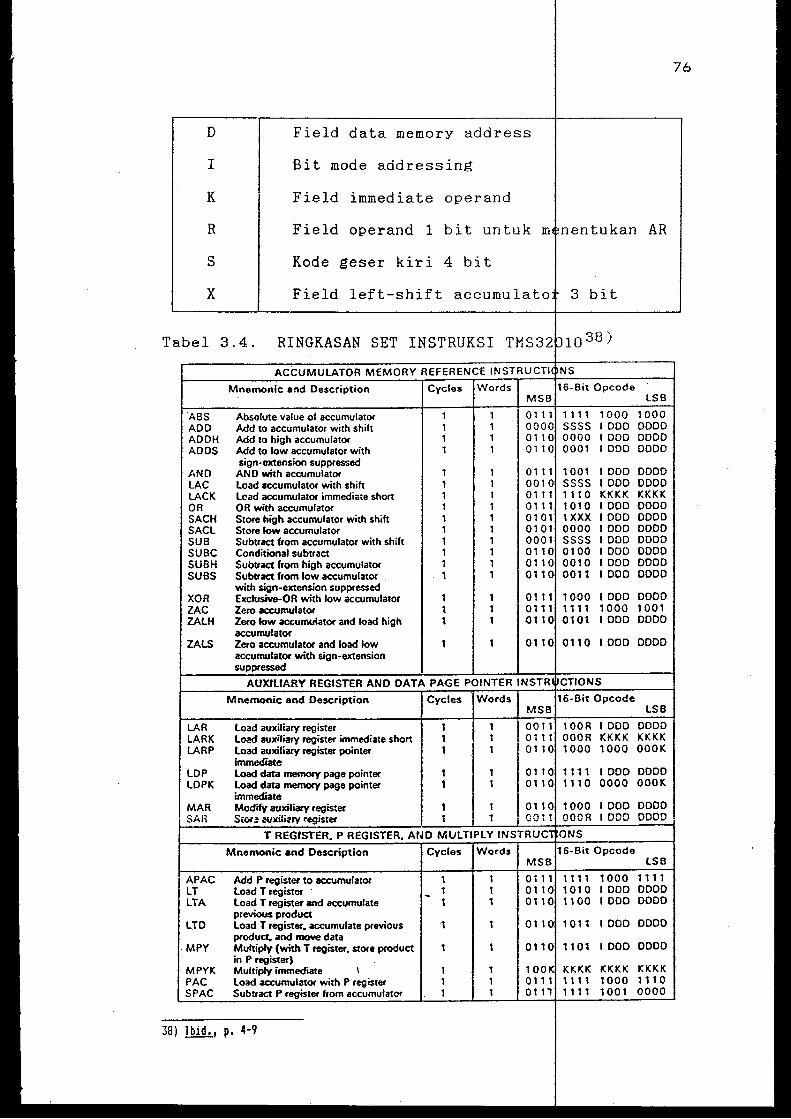
76
D Field data memory address
I Bit mode addressing
K Field immediate operand
R Field operand 1 bit untuk m nentukan AR
s Kode geser kiri 4 bit
X Field left-shift accumulate 3 bit
Tabel 3.4. RINGKASAN SET INSTRUKSI TMS32 1038)
LSB
ABS Absolute value of accumulator 1000 1000 ADD Add to accumulator with shift I ODD DODD ADDH Add to high accumulator I DOD 0000 ADDS Add to low accumulator with I 000 0000
sign-extension suppressed ,,No AND with accumulator 1 1 I 000 DODO LAC load accumulator with shift 1 1 I DOD DODD LACK load accumulator immediate short 1 1 KKKK KKKK OR OR with accumulator 1 1 I 000 DODO SACH Store high accumulator with shift 1 1 I 000 0000 SACL Store low accumulator 1 1 I ODD DODD SUB Subtract from accumulator with shift 1 1 I ODD DODD SUBC Conditional subtract 1 1 I ODD DODO SUBH Subtract from high accumulator 1 1 I ODD DODO SUBS Subtract from low accumulator 1 1 I ODD DODO
with sign-extension suppressed XOR Exclusive-OR with low accumulator I DOD DODD ZAC Zero accumulator 1000 1001 ZAlH Zero low accumulator and load high I DOD DODD
accumulator ZALS Zero accumulator and load low I DOD DODD
accumulator with sign-extension suppressed
LSB
LAR load auxiliary register I DOD 0000 LA.RK load auxiliary register immediate short KKKK KKKK LARP load auxiliary register pointer 1000 OOOK
irnme<ftate LOP load data memory page pointer I 000 DODO LDPK load data memory page pointer 0000 OOOK
immediate MAR Modify auxiliary register I DOD 0000 SAB Stor ~ ooxili;;ry register ! ODD ODOD
lSB
APAC Add P register to accumulator 1 1000 1111 LT load T register 1 I DOD DODO LTA load T register and accumulate 1 I ODD 0000
previous product LTD load T register. accumulate previous I ODD DODD
product. and move data MPY Multiply (with T register. store product I 000 0000
in P register) MPYK Multiply immediate 1 KKKK KKKK KKKK PAC load accumulator with P register 1 1111 1000 1110 SPAC Subtract P register from accumulator 1 1111 1001 0000
38) Ibid. I p. 4-9
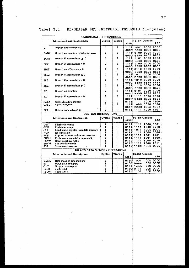
77
Tabel 3.4. RINGKASAN SET INSTRUKSI TMS3 10 ( lanjutan)
6-Bit Opcode LSB
B Branch unconditionally 2 2 1001 0000 0000 BBBB 6888 BBBB
BANZ Branch on awciliary register not zero 2 2 0100 0000 0000 BBBB 6868 8868
BGEZ Branch if accumulator 2: 0 2 2 1101 0000 0000 6688 8888 8888
BGZ Branch if accumulator > 0 2 2 1100 0000 0000 8888 8888 8888
BIOZ Branch on 1/0 status = 0 2 2 0110 0000 0000 BBBB BBB8 8888
BLEZ Branch if accumulator S 0 2 2 1011 0000 0000 8888 BBBB BBBB
BLZ Branch if accumulator < 0 2 2 1010 0000 0000 BBBB 8888 BBBB
BNZ Branch if accumulator Jl: 0 2 2 111 0 0000 0000 BBBB 6688 8866
BV Branch on overflow 2 2 0101 0000 0000 8888 BBB8 8888
BZ Branch if accumulator = 0 2 2 1 1 1 1 0000 0000 BBBB 6888 BBBB
CALA Call subroutine indirect 2 1 111 1 1000 1100 CALL Call subroutine 2 2 1000 0000 0000
BBBB BBBB BBBB RET Return from subroutine 11 1 1 1000 1101
6-Bit Opcoda MSB LSB
OINT Disable interrupt 1 1 0111 1111 1000 0001 EINT Enable interrupt 1 1 0111 1111 1000 0010 lST load status register from data memory 1 1 0111 1 01 1 I 000 0000 NOP No operation 1 1 0111 111 1 1000 0000 POP Pop top of stack to low accumulator 2 1 0111 1111 1001 1101 PUSH Push low accumulator onto stack 2 1 0111 1111 1001 1100 ROVM Reset overflow mode 1 1 0111 1111 1000 1010 SOVM Set overflow mode 1 1 0111 1111 1000 1011 SST Store status register 1 1 0111 1100 I 000 0000
6-Bit Opcode MSB LSB
DMOV Data move in data memory 1 0110 1001 I DOD DODD IN Input data from port 2 0100 OAAA I ODD DODD OUT Output data to port 2 0100 1AAA I ODD 0000 TBLR Table read 3 0110 0111 I ODD DODD TBLW Table write 3 0111 11 01 I DOD DODD
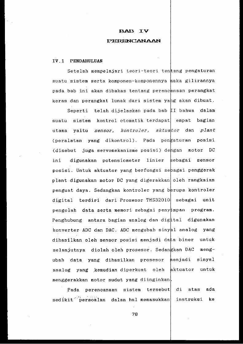
BAB IV
PERENC.ANAAN
IV.l PENDAHULUAN
Setelah mempelajari teori-teori ten pengaturan
suatu sistem serta komponen-komponennya gilirannya
pada bab ini akan dibahas tentang perenc naan perangkat
keras dan perangkat lunak dari akan dibuat.
Seperti telah dijelaskan pada bab bahwa dalam
suatu sistem kontrol otomatik terdapat empat bagian
utama yaitu sensor, kontroler, aktu dan plant
(peralatan yang dikontrol). Pada posisi
(disebut juga servomekanism~ posisi) de motor DC
ini digunakan potensiometer linier sensor
posisi. Untuk aktuator yang berfungsi se penggerak
plant digunakan motor DC yang digerakkan rangkaian
penguat daya. Sedangkan kontroler yang b kontroler
digital terdiri dari Prosesor TMS32010 sebagai unit
pengolah data serta memori sebagai pen an program.
I
antara bagian analog dan dig tal digunakan Penghubung
konverter ADC dan DAC. ADC mengubah sin analog yang
I
dihasilkan oleh sensor posisi menjadi da a biner untuk
selanjutnya diolah oleh prosesor. Sedan meng-
ubah data yang dihasilkan prosesor sinyal
analog yang .kemudian diperkuat oleh untuk
menggerakkan motor sudut yang diinginkan
Pada perencanaan sistem tersebut di atas ada
.~ • • • >~ • . : , ~ I
sed1k1t persoalan dalam hal memasukkan instruksi ke
78
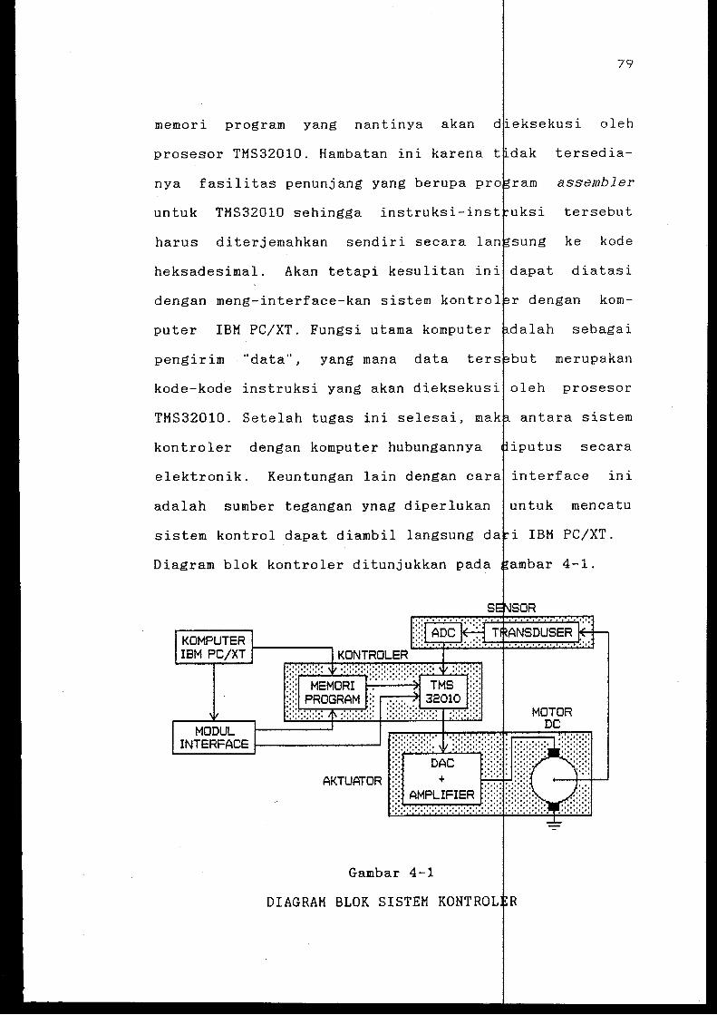
79
memori program yang nantinya akan oleh
prosesor TMS32010. Hambatan ini karena tersedia-
nya fasilitas penunjang yang berupa pro assembler
untuk TMS32010 sehingga instruksi-inst tersebut
harus diterjemahkan sendiri secara ke kode
heksadesimal. Akan tetapi kesulitan ini diatasi
dengan meng-interface-kan sistem kontrol r dengan kom-
puter IBM PC/XT. Fungsi utama komputer alah sebagai
pengirim "data", yang mana data merupakan
TMS32010. Setelah tugas ini selesai, mak antara sistem
kontroler dengan komputer hubungannya secara
elektronik. Keuntungan lain dengan cara interface ini
adalah sumber tegangan ynag diperlukan untuk mencatu
sistem kontrol dapat diambil langsung da
Diagram blok kontroler ditunjukkan pada
KOMPUTER 1-------. IBM PC/XT
AKTUATOR
Gambar 4-1
DIAGRAM BLOK SISTEM KONTROL R
PC/XT.
4-1.
80
IV.2 SLOT PERIPHERAL IBM PC/XT I
Sebelum menginjak lebih lanjut p a perencanaan
sistem kontroler, baiklah lebih dahulu akan dibahas
tentang slot peripheral pada IBM PC/XT, karena untuk
dapat meng-interface-kan suatu sistem d ngan komputer
harus diketahui dengan pasti letak pin- in dan fungsi
masing-masing dari slot peripheral IBM P /XT.
Seperti ditunjukkan pada gambar 4- slot peri-
pheral IBM PC/XT terdiri dari 62 pin. Sinyal-sinyal
tersebut dapat dijelaskan sebagai beriku
OSC (Oscillator)
Sinyal ini merupakan sinyal output engan frekuen-
si 14,31818 MHz dan perioda sekitar 70 ns.
Duty cycle kira-kira 50%. Sinyal ini merupakan
sinyal frekuensi tertinggi pada bu dan seluruh
sinyal pada sistem dibangkitkan ole sinyal ini.
CLK <Clock)
Sinyal ini diambil dari sinyal 0 yang dibagi
tiga sehingga mengeluarkan freku si 4,77 MHz.
Sinyal CLK tidak simetris, kan mempunyai
duty cycle sepertiga/duapertiga. sinyal
ini 210 ns dengan waktu level high 0 ns dan waktu
level low 140 ns.
RESET DRY <Reset Driver)
Sinyal ini mengeluarkan sinyal akt f high selama I
proses system power-on dan tetap aktif sampai
seluruh sistem mencapai level opera i yang diten-'
tukan, kemudian sinyal ini tidak ak if (low).
81
AO-A19
D0-07
Bit address AO-A19 digunakan untuk address memori I
dan I/0. Ke-20 sinyal ini diaktif an oleh mikro-
prosesor 8088 untuk menunjuk pad address yang
dituju selama read cycle atau wri e cycle memori
dan I/0.
Kedelapan jalur data dua arab (bid rectional) ini
digunakan untuk mentransfer data antara mikro-
prosesor 8088, memori dan I/0.
ALE (Address Latch Enable)
Sinyal output ini diaktifkan dari bus controller
8288. Ini digunakan untuk aenunju an bahwa bus
address berlaku untuk permulaan s bus cycle.
Sinyal ini menjadi aktif high ses t sebelum bus
address stabil. Sinyal ini digun kan untuk me-
latch informasi alamat dari bus ad ress/data lokal
dari mikroprosesor 8088.
I/0 CH CK CI/0 Channel Check)
Sinyal input level low ini digun an untuk mem-
beritahukan kondisi error pada bu yang berasal
dari interface card. Sinyal ini ila diset low
akan membangkitkan nonmaskable nterrupt (NMI)
pada mikroprosesor 8088.
I/0 CH RDY CI/0 Channel Ready)
Sinyal input ini digunakan untu memperpanjang
waktu bus cycle, sehingga memori atau port I/0
82
yang memiliki respon lebih lamba daripada bus
cycle normal empat clock (840 n ) masih dapat
dihubungkan dengan bus sistem. Ji a suatu memori
atau port I/0 perlu memperpanjang bus cycle, ia
harus memberikan sinyal low pada I CH RDY ketika
ia men-decode address tersebut dan suatu
instruksi MEMR, HEMW, IOR atau I Sinyal ini
harus dikontrol dengan hati-hati sehingga hanya
diperlukan saat kondisi menunggu (
Keenam sinyal input ini digunakan untuk membang-
kitkan interrupt request ke mik oprosesor 8088
dari bus sistem. Sinyal-sinyal te sebut langsung
menuju interrupt controller 8259A Program BIOS
menginisialisasi 8259A sehingga IRQ2 merupakan
prioritas tertinggi dan IRQ7 tere ah.
IOR (I/0 Read)
Sinyal ini merupakan sinyal output aktif low , yang
berasal dari bus controller 8288. Ini digunakan
untuk memberitahu pada port I/0 bus cycle
yang dilakukan 8088 adalah read dari port
I/0 dan address pada bus address m rupakan address I
port I/0.
row <I/O Write)
Sinyal ini merupakan sinyal outpu aktif low. Ia
juga diaktifkan oleh 8288 dan me 1
unjukkan bahwa
bus address merupakan address po t I/0 dan bus
data berisi data yang akan ditulis ke port I/0.
83
Sinyal ini aktif low digunakan unt k menulis data
dari bus sistem ke memori. Sinyal lini digerakkan
oleh bus controller 8288 yang m unjukkan bahwa I
bus address berisi address lokasi I memori tempat
data akan ditulis.
Sinyal ini aktif low digunakan unt k membaca data
dari memori. Ia juga digerakkan leh 8288 yang
menunjukkan bahwa bus alamat beris address lokasi I
memori yang ditunjuk untuk dibaca.
through 3)
Ketiga jalur ini adalah input akti high digunakan
oleh interface untuk DMA regue t. Jika suatu
peralatan atau interface ingin m ntransfer data
antara dirinya dengan memori secar langsung tanpa
melibatkan mikroprosesor 8088, ma a DMA request
dimulai dengan memberikan sinyal level high ke
jalur DRQ. Jalur ini berhubungan angsung ke DMA
controller 8237-5. Program pada M BIOS meng-
inisialisasi sehingga DRQl meru akan prioritas
tertinggi dan DRQ3 terendah. S benarnya yang
memiliki- prioritas tertinggi ada ah DRQO, akan
tetapi ini tidak disediakan pada s sistem. DRQO
digunakan sistem komputer untuk me1refresh memori
!
dinamik.
84
through 32
Keempat sinyal ini mempunyai outpu aktif low yang
digunakan oleh 8237-5 untuk menunj kkan bahwa DRQ
telah diterima dan DMA controller akan mengguna
kan bus serta meneruskan cycle DHA yang diminta.
AEN ( Address Enable)
Sinyal ini merupakan output aktif yang digu-
nakan oleh DHA controller logic. i menunjukkan
bahwa DHA bus cycle sedang berlang ung. Sinyal ini
juga digunakan untuk melepas h ungan bus-bus
address, data dan kontrol mikropro esor 8088 dari
bus sistem dan mengaktifkan addre kon
trol dari DHA controller.
TC (Terminal Count)
Sinyal output ini aktif high digu oleh DHA
controller 8237-5. Sinyal ini m njukkan bahwa
salah satu dari kanal DHA telah
cycle transfer yang direncanak
khususnya digunakan untuk
data blok DHA.
+5 Y DC
jumlah
Sinyal ini
transfer
Level tegangan +5 volt tersedia pada dua pin
konektor slot dan mempunyai toler i ± 5% (+4,75
hingga +5,25 volt de).
+12 Y DC
Level tegangan +12 volt tersedia p a satu pin de
ngan toleransi ± 5% (+11,4 hingga 2,6 volt de).
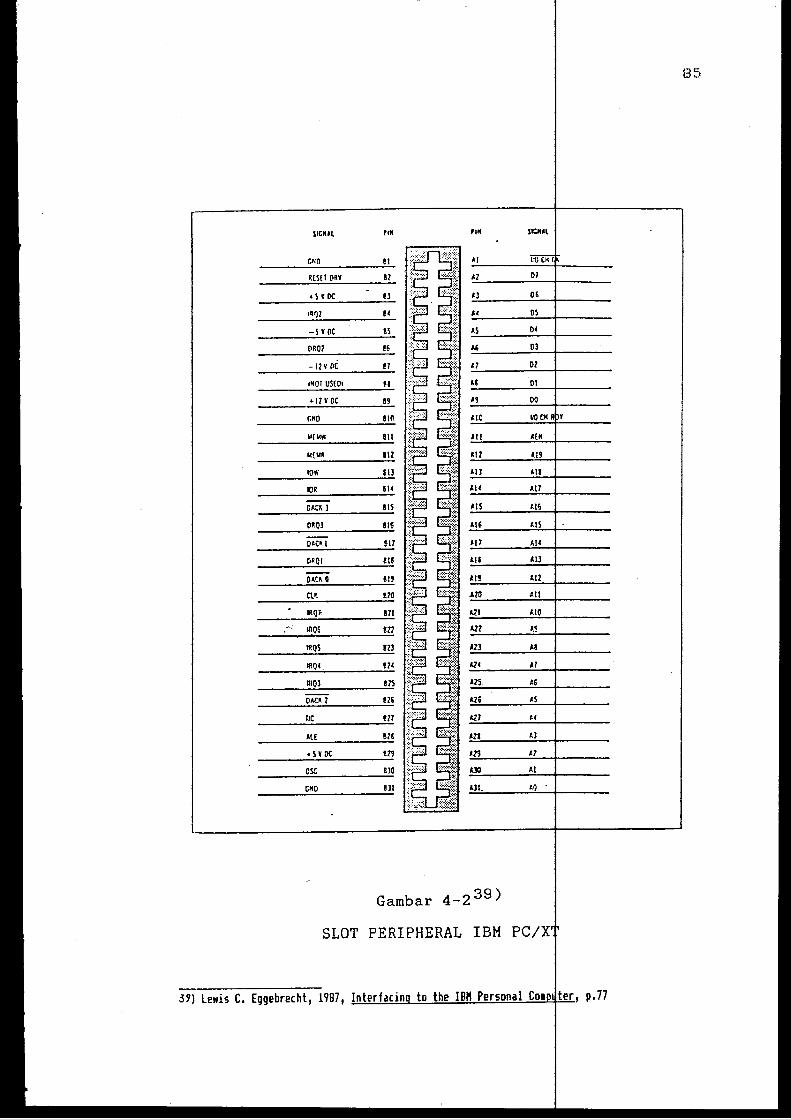
85
SICM&l '"' fill SIOI&l
CNO 81
R[S£1 ORV 81
•HOC Bl
·q~l 81
-I¥ DC 85
OROl !6
-12VOC !I
oN01 USED• u + 12 V DC 89
tHO 810
tol(lol ... 811
lol[toiF. m lOW m lOR 111
OAC~ l !IS
OROl 816
OACi.1 517
DRQI au
ll&C~ 0 m
ct'- 610
IRQ> 811
mos en II!QS m
II!QI. !lC
AIQJ 8lS
OACJ\2 m
TIC 827
AlE 82&
•HOC 81!
osc 8)0
CHO !J1
Gambar 4-2 39 )
SLOT PERIPHERAL IBM
39) lewis C. Eggebrecht, 1987, p.77
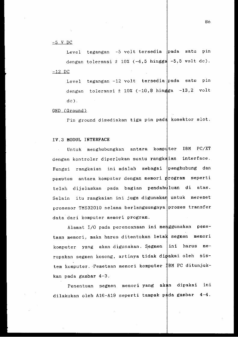
86
-5 V DC
Level tegangan -5 volt tersedia pada satu pin
dengan toleransi ± 10% (-4,5 hingg -5,5 volt de).
-12 DC
Level tegangan -12 volt tersedia pada satu pin
dengan toleransi ± 10% (-10,8 hi -13,2 volt
de).
GND (Ground)
Pin ground disediakan tiga pin pad konektor slot.
IV.3 HODUL INTERFACE
Untuk menghubungkan antara
dengan kontroler diperlukan suatu
ter IBM PC/XT
ian interface.
Fungsi rangkaian ini adalah sebagai penghubung dan
pemutus antara komputer dengan memori rogram seperti
telah dijelaskan pada bagian di atas.
Selain itu rangkaian ini juga diguna untuk mereset
prosesor TMS32010 selama berlangsungnya proses transfer
data dari komputer memori program.
Alamat I/0 pada perencanaan ini ggunakan peme-
taan memori, maka harus ditentukan let segmen memori
komputer yang akan digunakan. ~egmen ini harus me-
rupakan segmen kosong, akai oleh sis-
tem komputer. ~emetaan memori komputer BM PC ditunjuk
kan pada gambar 4-3.
Penentuan segmen memori yang dipakai ini
dilakukan oleh A16-A19 seperti tampak p a gambar 4-4.
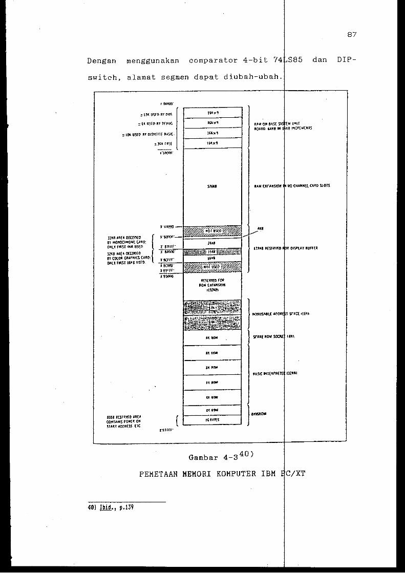
Dengan menggunakan comparator 4-bit 74 S85 dan
switch, alamat segmen dapat diubah-ubah.
, on<!OO"
= 17~ 11510 RY !10~
RAil ON SASE ttNII ROARO '4K8 IN R I~O'("'[NIS
= IOk USf[' RY DISk! liE ~~SIC·
51~ RAil (lrAIISION 110 (IWI!Itl CARD SlOTS.
ll~R AREA OECOntO ( 81 IIOHOCIIOOU( CACO: OHtT llt!ST «U U$[0
32~~ ARE A OECOOE 0 { SY COlOR curHICS CA«O: OHlT fi1!ST 15•8 IISfO
IOU RESfRI"fO AR(A COH!AIHS rowt'- OH ~TART AOORESS {IC.
,._
{ ]·-nrrrr·
Gambar 4-3 40 )
PEMETAAN HEMORI KOMPUTER IBM
40) Ibid., p.139
/XT
87
DIP-
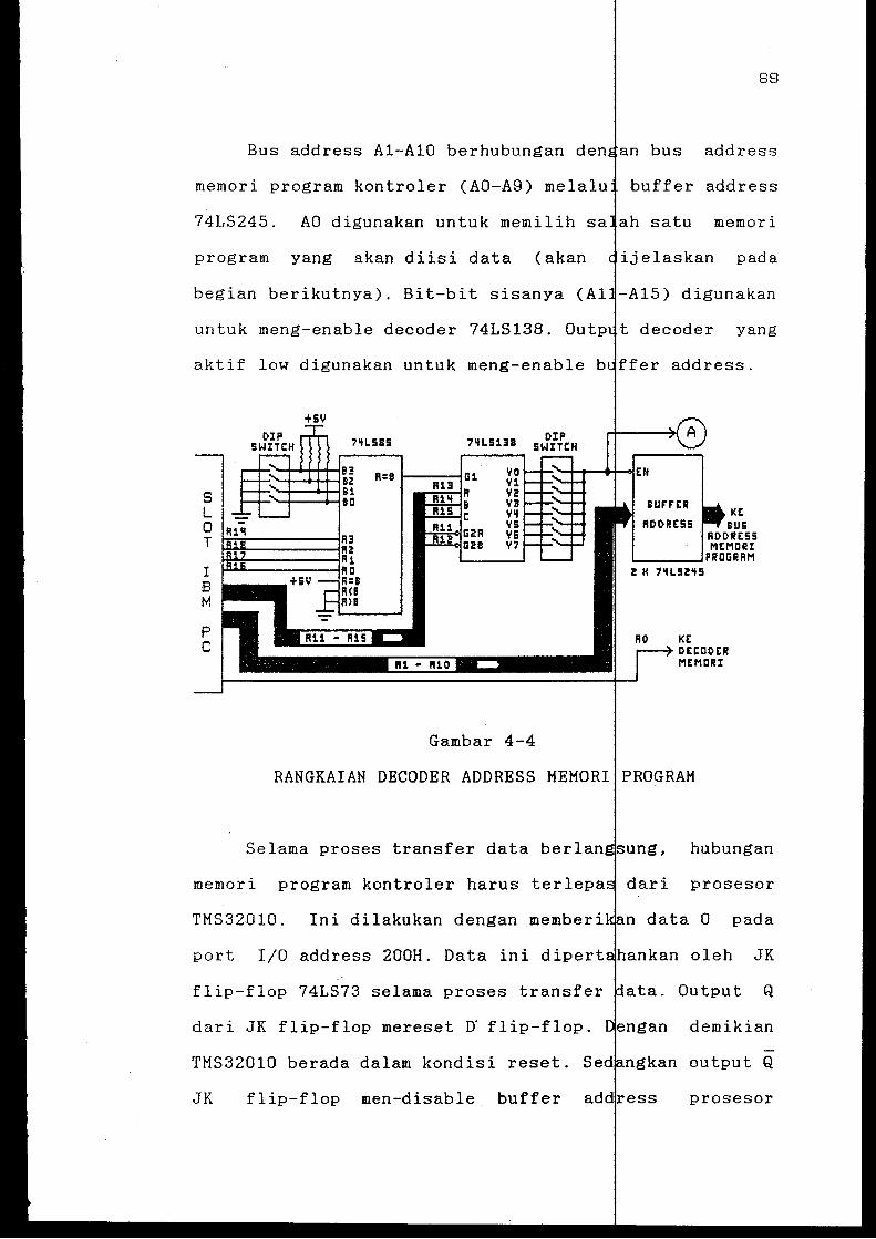
88
Bus address Al-AlO berhubungan den an bus address I
memori program kontroler (AO-A9) melalu buffer address
74LS245. AO digunakan untuk memilih sa ah satu memori
program yang akan diisi data (akan ij e laskan pad a
begian berikutnya). Bit-bit sisanya (Al ~-A15) digunakan
untuk meng-enable decoder 74LS138. Outp t decoder yang
aktif low digunakan untuk meng-enable b ffer address.
+SV
y 0 ~-: '-f-<r--+il--ol £ Y1 y 2 '----'--'-~ Y! Ylf L-...1.-'-...L...I. y s '----'--'-~ VIi y 7 '----'--'--L-1
Gambar 4-4
2 K 71fL52'+5
K£ OECDD£11 MEMDRI
RANGKAIAN DECODER ADDRESS MEMORI PROGRAM
Selama proses transfer data berl hubungan
memori program kontroler harus prosesor
TMS32010. Ini dilakukan dengan memberi pad a
port I/0 address 200H. Data ini dipert kan oleh JK
flip-flop 74LS73 selama proses transfer Output Q
dari JK flip-flop mereset rr flip-flop. demikian
TMS32010 berada dalam kondisi reset. output Q
JK flip-flop men-disable. buffer prosesor
89
TMS32010. Setelah transfer data selesai ilakukan maka
port I/0 address 200H diberi data 1 sehi JK
flip-flop menjadi Q="l" dan Q="O". Kendi ini membuat
prosesor TMS32010 mulai bekerja dan address-nya
terhubung dengan bus address memori Rangkaian
ini ditunjukkan pada gambar 4-5.
7'1L527 7'1L513S
KE PIN liST TM5:U010
I<E PIN ENABLE 7'1L52'10
V?
ORRI PIN C:LKDUT TMS32010
:J
C:LI<
K I<E PIN ENABLE BUFf"ER ROOR£55 TM5:!12010
POWER ON RESET -
Gambar 4-5
RANGKAIAN ISOLASI TMS3201
DENGAN MEMORI PROGRAM
Bus data komputer IBM PC/XT ada sedangkan
prosesor TMS32010 memiliki 16-bit data. Untuk
mengubah bus data dari 8-bit dilakukan
dengan menggunakan dua buah buffer yang pada
input-inputnya dihubungkan paralel, sed kan outputnya
dihubungkan dengan masing-masing bus da dari kedua
memori program (lihat gambar 4-6). er-buffer ini
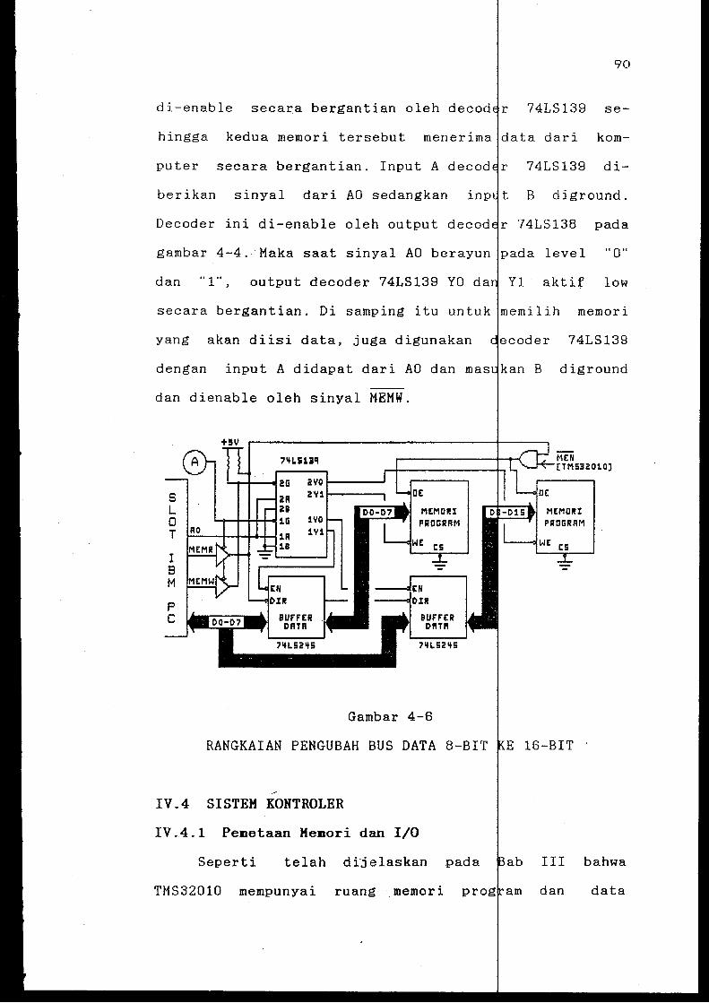
90
di-enable secara bergantian oleh decod lr 74LS139 se-
hingga kedua memori tersebut menerima kom-
puter secara bergantian. Input A decod r 74LS139 di
berikan sinyal dari AO sedangkan inp B diground.
Decoder ini di-enable oleh output decod r 74LS138 pada
gambar 4-4. Maka saat sinyal AO berayun level "0"
dan "'1"', output decoder 74LS139 YO da Y1 aktif low
secara bergantian. Di samping itu untuk memori
yang akan diisi data, juga digunakan coder 74LS139
dengan input A didapat dari AO dan mas diground
dan dienable oleh sinyal MEMW.
Gambar 4-6
RANGKAIAN PENGUBAH BUS DATA 8-BIT
IV.4 SISTEH KONTROLER
IV .. 4 .1 Pemetaan Hemori dan I/0
Seperti telah dijelaskan pada
TMS32010 mempunyai ruang memori pr
16-BIT ·
ab III bahwa
am dan data
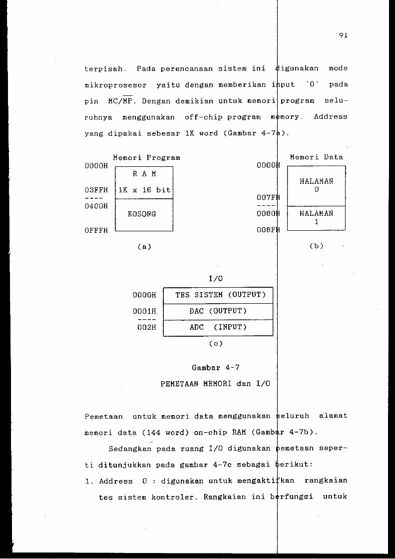
terpisah. Pada perencanaan sistem ini
mikroprosesor yaitu dengan memberikan
pin MC/MP. Dengan demikian untuk memori
ruhnya menggunakan off-chip program
yang dipakai sebesar lK word (Gambar 4-7
OOOOH
03FFH
0400H
OFFFH
Memori Program
R A M
1K X 16 bit
KOSONG
(a)
OOOOH
0001H
002H
0000
008
I/0
TES SISTEM (OUTPUT)
DAC (OUTPUT)
ADC (INPUT)
(c)
Gambar 4-7
PEMETAAN MEMORI dan I/0
91
igunakan mode
'0' pad a
selu-
ry. Address
Memori Data
HAL AM AN 0
HAL AM AN 1
(b)
Pemetaan untuk memori data menggunakan eluruh alamat
memori data (144 word) on-chip RAM (Gamb r 4-7b).
I
Sedangkan pada ruang I/0 digunakan emetaan seper-
ti ditunjukkan pada gambar 4-7c sebagai erikut:
1. Address 0 : digunakan untuk mengakti kan rangkaian
tes sistem kontroler. Rangkaian ini b rfungsi untuk
92
menguji apakah prosesor dan rangkai output sudah I
bekerja dengan baik. Rangkaian tes in terdiri dari
sebuah data latch 8 bit 74LS373 dan 8 buah LED.
Dengan mengirimkan data 8 ress ini akan
diketahui bahwa bila LED menyala i dengan bit-
bit data yang dikirimkan berarti sor dan rang-
kaian output bekerja dengan baik.
2. Address 1 : digunakan untuk mengir an data dari
prosesor TMS32010 ke DAC melalui data latch 74LS374.
3. Address 2 : digunakan untuk mengambi data dari ADC
yang merupakan hasil konversi teg analog yang
didapat dari transduser potensiometer
IV.4.2 Decoding
Decoding berfungsi untuk men-decode jalur address
prosesor untuk mengaktifkan memori ata piranti I/0
agar data yang dikirim ke atau diterima dari piranti
tersebut tidak kacau.
Dari pemetaan memori di atas tamp bahwa untuk
memori tidak perlu dilakukan decoding arena seperti
telah dijelaskan bahwa ruang untuk memo i program dan
memori data memang terpisah. Dekoding di erlukan hanya
pada address I/0 yang nanti akan menentu an piranti I/0
mana yang akan diaktifkan. !
Pada gambar 4-8 ditunjukkan cara! menghubungkan
prosesor dengan memori program ekste nal. I
Prosesor
TMS32010 memiliki bus data 16 bit, sed kan di pasaran
tidak ada/sulit didapatkan memori yang memiliki bus
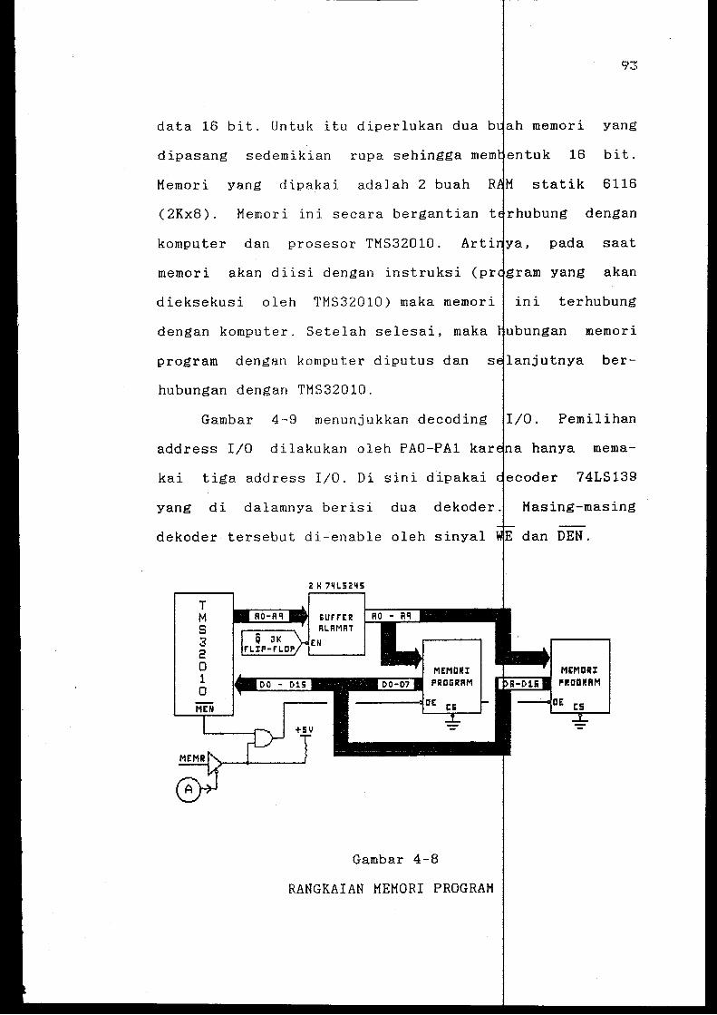
93
data 16 bit. Untuk itu diperlukan dua b memori yang
dipasang sedemikian rupa sehingga mem 16 bit.
Memori yang dipakai adalah 2 buah R statik 6116
(2Kx8). Memori ini secara bergantian t rhubung dengan
komputer dan prosesor TMS32010. Arti a, pada saat
memori akan diisi dengan instruksi (pr yang akan
dieksekusi oleh TMS32010) maka memori ini terhubung
dengan komputer. Setelah selesai, maka ubungan memori
program dengan komputer diputus dan s lanjutnya ber-
hubungan dengan TMS32010.
Gambar 4-9 menunjukkan decoding I/0. Pemilihan
address I/0 dilakukan oleh PAO-PA1 kar a hanya mema-
kai tiga address I/0. Di sini dipakai 74LS139
yang di dalamnya berisi dua dekoder. Masing-masing
dekoder tersebut di-enable oleh sinyal
T M s 3 2 0 1 0
2 H ?'ILS2'15
Gambar 4-8
RANGKAIAN MEMORI PROGRAM
dan DEN.
PI!DGRRM
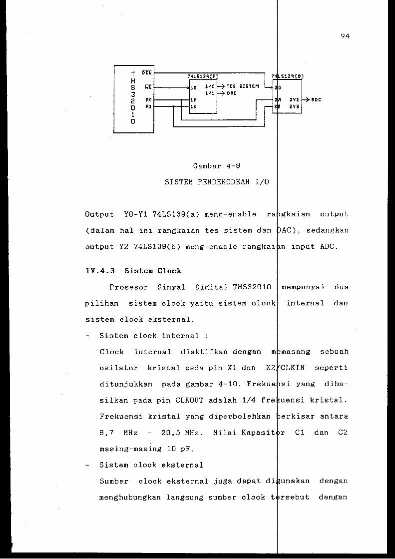
94
T m M s WE TES SISTEM
3 OAt:
2 AO 1A A DC:
0 A1 8
1 0
Gambar 4-9
SISTEH PENDEKODEAN I/0
Output YO-Yl 74LS139(a) meng-enable r gkaian output
(dalam hal ini rangkaian tes sistem dan AC), sedangkan
output Y2 74LS139(b) meng-enable rangkai n input ADC.
IV.4.3 Sistem Clock
Prosesor Sinyal Digital TMS32010 , mempunyai dua
pilihan sistem clock yaitu sistem clock internal dan
sistem clock eksternal.
Sistem clock internal
Clock internal diaktifkan dengan sebuah
osilator kristal pada pin Xl dan seperti
ditunjukkan pada diha-
Frekuensi kristal yang diperbolehkan erkisar antara
6,7 MHz 20,5 MHz. Cl dan C2
masing-masing 10 pF .
. Sistem clock eksternal
Sumber clock eksternal juga dapat di nakan dengan
menghubungkan langsung sumber clock t dengan
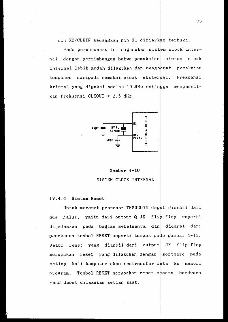
95
pin X2/CLKIN sedangkan pin Xl dibiar terbuka.
Pada perencanaan ini digunakan sis clock inter-
nal dengan pertimbangan bahwa pemakaian sistem clock
internal lebih mudah dilakukan dan meng
komponen daripada memakai clock
kristal yang dipakai adalah 10 MHz sehi
kan frekuensi CLKOUT = 2,5 MHz.
1opr I
T M s 3
....-..1..----1 H 21 2 CLKIN 0
1opr I
Gambar 4-10
1 0
SISTEM CLOCK INTERNAL
IV.4.4 Sistem Reset
Untuk mereset prosesor TMS32010
dua jalur, yaitu dari output Q JK
dijelaskan pada bagian sebelumnya
pemakaian
Frekuensi
menghasil-
t diambil dari
-flop seperti
didapat dari
penekanan tombol RESET seperti tampak p a gambar 4-11.
Jalur reset yang diambil dari output JK flip-flop
merupakan reset yang dilakukan dengan 1 software pada
setiap kali komputer akan mentransfer ta ke memori
program. Tombol RESET merupakan reset hardware
yang dapat dilakukan setiap saat.
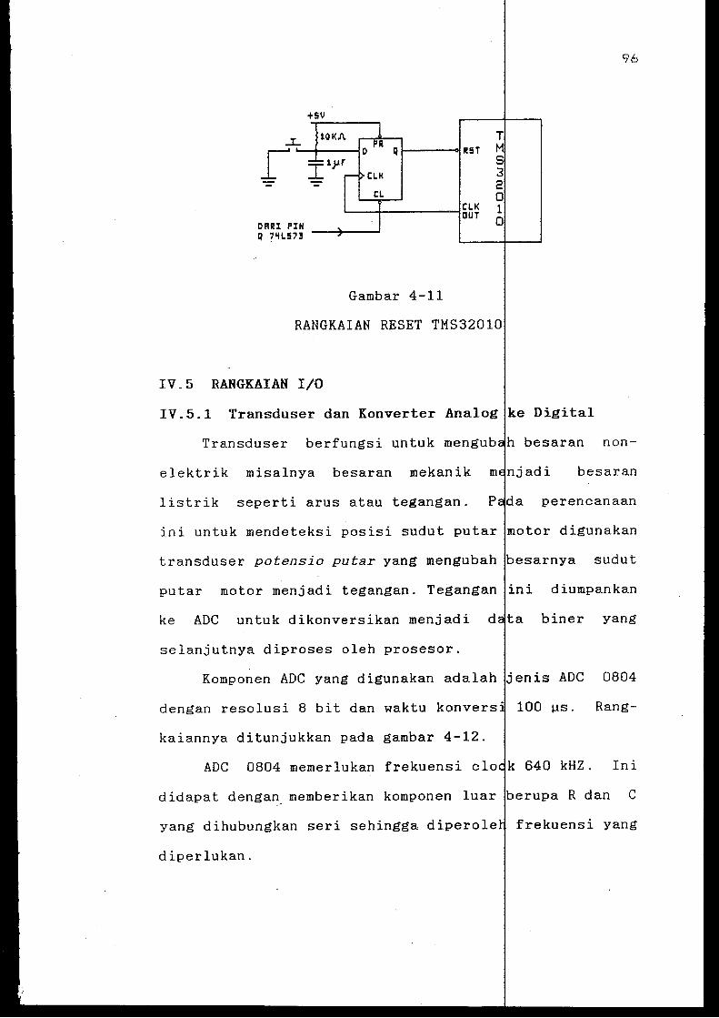
96
+SV
..L _r g li!ST
- - CL C:LK OUT
DRRI PIN Q ?lfLS?!
Gambar 4-11
RANGKAIAN RESET TMS32010
IV.5 RANGKAIAN I/0
IV.5.1 Transduser dan Konverter Analog ke Digital
Transduser berfungsi untuk mengub non-
elektrik misalnya besaran mekanik be saran
listrik seperti arus atau tegangan. P a perencanaan
ini untuk mendeteksi posisi sudut putar motor digunakan
transduser potensio putar yang mengubah esarnya sudut
putar motor menjadi tegangan. Tegangan diumpankan
ke ADC untuk dikonversikan menjadi d a biner yang
selanjutnya diproses oleh prosesor.
Komponen ADC yang digunakan adalah enis ADC 0804
dengan resolusi 8 bit dan waktu konvers 100 ~s. Rang-
kaiannya ditunjukkan pada gambar 4-12.
ADC 0804 memerlukan frekuensi clo Ini
didapat denga~ memberikan komponen luar erupa R dan C
yang dihubungkan seri sehingga diperole frekuensi yang
diperlukan.
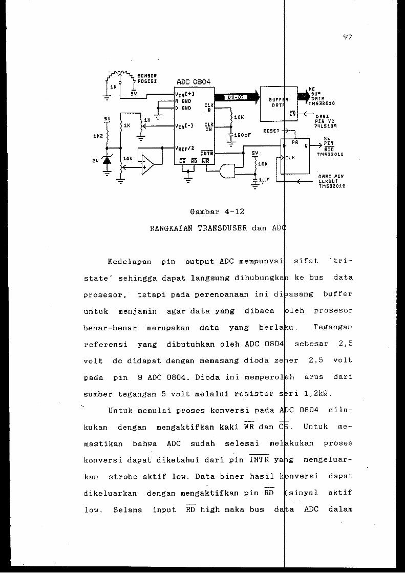
2V
Gambar 4-12
RANGKAIAN TRANSDUSER dan AD
1<!: PIN rn
TM532010
97
ORRI PIN C:LI<OUT TM532010
Kedelapan pin output ADC mempunyai sifat 'tri-
state' sehingga dapat langsung dihubungk 1
ke bus data
prosesor, tetapi pada perencanaan ini di buffer
untuk menjamin agar data yang dibaca prosesor
benar-benar merupakan data yang Tegangan
referensi yang dibutuhkan oleh ADC 08 sebesar 2,5
volt de didapat dengan memasang 2,5 volt
pada pin 9 ADC 0804. Dioda ini mempero arus dari
sumber tegangan 5 volt melalui resistor 1,2kQ.
Untuk memulai proses konversi pada 0804 dila-
kukan dengan mengaktifkan kaki WR dan Untuk me-
mastikan bahwa ADC sudah selesai proses
konversi dapat diketahui dari pin mengeluar-
kan strobe aktif low. Data biner hasil dapat
dikeluarkan dengan mengaktifkan pin RD aktif
low. Selama input RD high maka bus ADC dalam
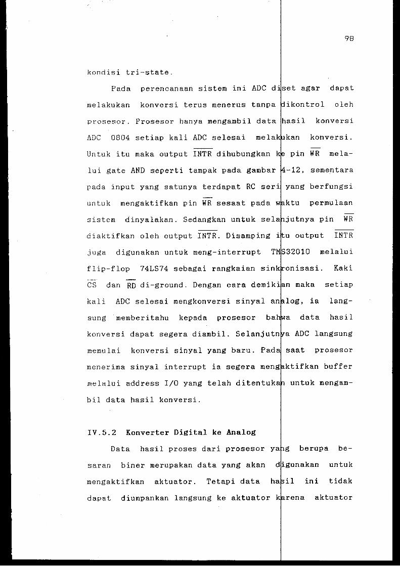
kondisi tri-state.
Pada perencanaan sistem ini
melakukan konversi terus menerus
prosesor. Prosesor hanya mengambil
ADC 0804 setiap kali ADC selesai
Untuk itu maka output INTR dihubungkan
98
dapat
ikontrol oleh
konversi
konversi.
pin WR mela-
lui gate AND seperti tampak pada gambar -12, sementara
pada input yang satunya terdapat
untuk mengaktifkan pin WR sesaat pada
berfungsi
permulaan
sistem dinyalakan. Sedangkan untuk sel jutnya pin WR
diaktifkan oleh output INTR. Disamping INTR
juga digunakan untuk meng-interrupt
flip-flop 74LS74 sebagai rangkaian sin
CS dan RD di-ground. Dengan cara demik
kali ADC selesai mengkonversi sinyal an
sung memberitahu kepada prosesor
konversi dapat segera diambil. Selanjutn
memulai konversi sinyal yang baru. Pad
melalui
onisasi. Kaki
setiap
lang
data hasil
ADC langsung
prosesor
menerima sinyal interrupt ia segera men ktifkan buffer
melalui address I/0 yang telah ditentuk untuk mengam
bil data hasil konversi.
IV.5.2 Konverter Digital ke Analog
Data hasil proses dari prosesor y
saran biner merupakan data yang akan
mengaktifkan aktuator. Tetapi data h
dapat diumpankan langsung ke aktuator
berupa be
untuk
ini tidak
aktuator
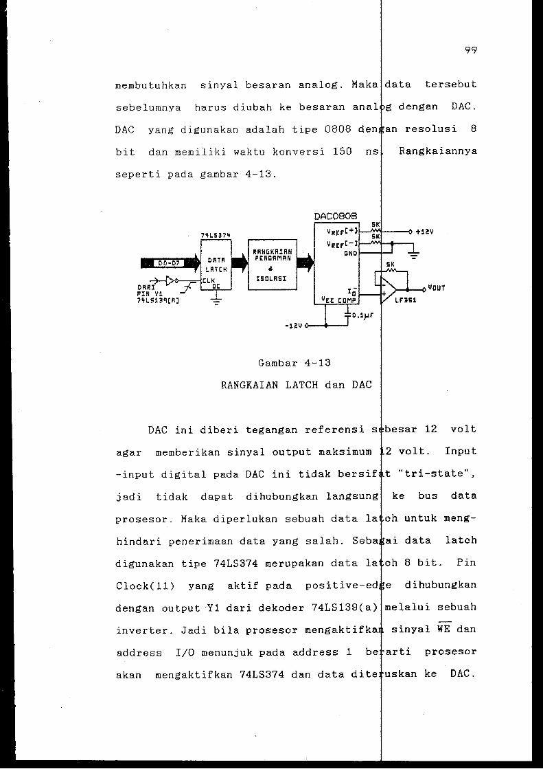
99
membutuhkan sinyal besaran analog. Maka data tersebut
sebelumnya harus diubah ke besaran anal g dengan DAC.
DAC yang digunakan adalah tipe 0808 den an resolusi 8
bit dan memiliki waktu konversi 150 ns
seperti pada gambar 4-13.
RRNGI<RIRN PENGRMRN
It
ISCLRSI
Gambar 4-13
RANGKAIAN LATCH dan DAC
Rangkaiannya
DAC ini diberi tegangan referensi s besar 12 volt
agar memberikan sinyal output maksimum 2 volt. Input
-input digital pada DAC ini tidak bersif t "tri-state",
jadi tidak dapat dihubungkan langsung ke bus data
prosesor. Maka diperlukan sebuah data la ch untuk meng-
hindari penerimaan data yang salah. Seb ai data latch
digunakan tipe 74LS374 merupakan data la ch 8 bit. Pin
Clock(ll) yang aktif pada positive-ed e dihubungkan
dengan output Yl dari dekoder 74LS139(a) melalui sebuah
inverter. Jadi bila prosesor mengaktif sinyal WE dan
address I/0 menunjuk pada address 1 be arti prosesor
akan mengaktifkan 7415374 dan data dite uskan ke DAC. I
I
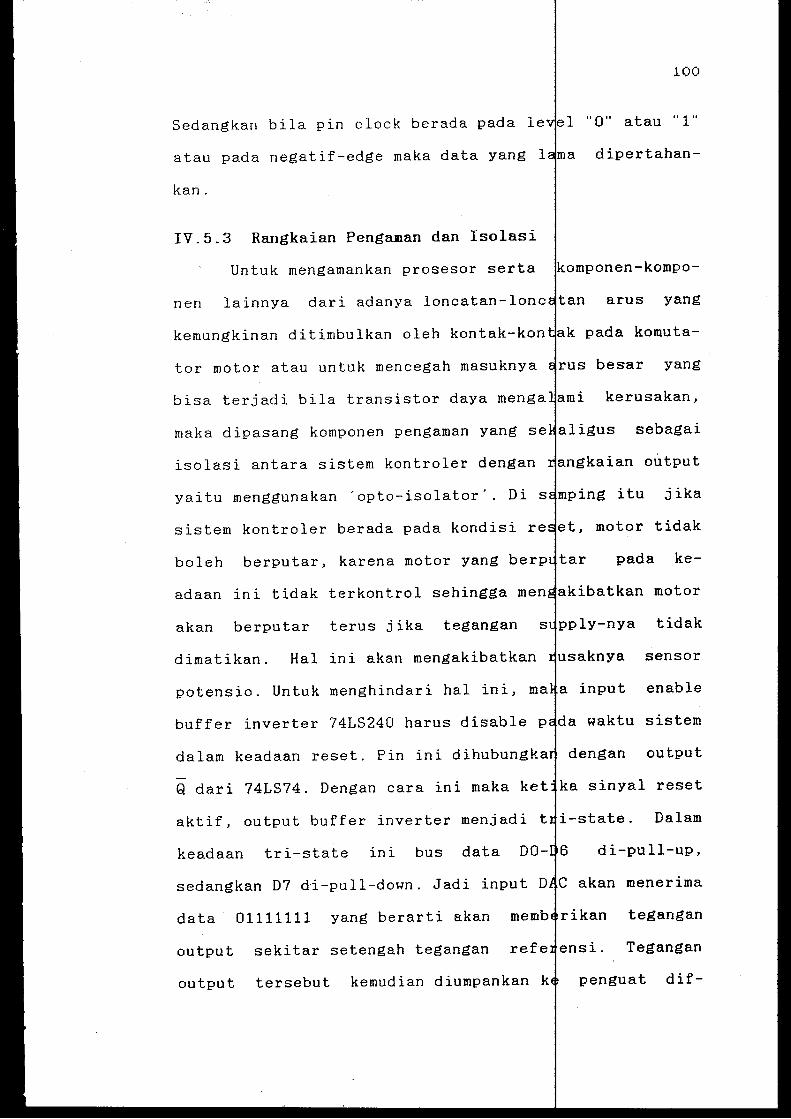
100
Sedangkan bila pin clock berada pada 1 1 "0" atau "1"
atau pada negatif-edge maka data yang 1 a dipertahan
kan.
IV.5.3 Rangkaian Penganan dan Isolasi
Untuk mengamankan prosesor serta
nen lainnya dari adanya loncatan-lonc
kemungkinan ditimbulkan oleh kontak-kon
tor motor atau untuk mencegah masuknya
bisa terjadi bila transistor daya menga
maka dipasang komponen pengaman
isolasi antara sistem kontroler dengan
yaitu menggunakan 'opto-isolator'. Di s
sistem kontroler berada pada kondisi re
boleh berputar, karena motor yang ber
adaan ini tidak terkontrol sehingga men
omponen-kompo
arus yang
k pada komuta
besar yang
i kerusakan,
sebagai
ngkaian output
ing itu jika
motor tidak
pada ke
motor
akan berputar terus jika tegangan tidak
dimatikan. Hal ini akan mengakibatkan usaknya sensor
potensio. Untuk menghindari hal ini, m
buffer inverter 74LS240 harus disable p
enable
sistem
dalam keadaan reset. Pin ini dihubungk dengan output
Q dari 74LS74. Dengan cara ini maka ket reset
aktif, output buffer inverter menjadi t i-state. Dalam
keadaan tri-state ini bus data DO- di-pull-up,
sedangkan 07 di-pull-down. Jadi input D akan menerima
data 01111111 yang berarti akan
output sekitar setengah tegangan
output tersebut kemudian diumpankan
tegangan
Tegangan
penguat dif-
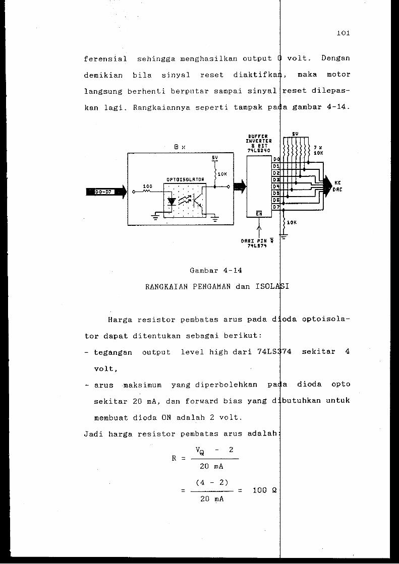
101
ferensial sehingga menghasilkan output volt. Dengan
demikian bila sinyal reset diaktifk maka motor
langsung berhenti berputar sampai sinyal reset dilepas-
kan lagi. Rangkaiannya seperti tampak p a gambar 4-14.
8 H
sv
10K
BUHER INVEI!TEii!
ll BIT ?'tLSi'IO
DRU PIN ij ?'tLS?'t
Gambar 4-14
RANGKAIAN PENGAMAN dan IS I
KE I>Rt
Harga resistor pembatas arus pada d oda optoisola-
tor dapat ditentukan sebagai berikut:
- tegangan output level high dari 74 sekitar 4
volt,
- arus maksimum yang diperbolehkan p a dioda opto
sekitar 20 mA, dan forward bias yang d butuhkan untuk
membuat dioda ON adalah 2 volt.
Jadi harga resistor pembatas arus adalah
2 R =
20 rnA
(4 - 2) = = 100 Q
20 rnA
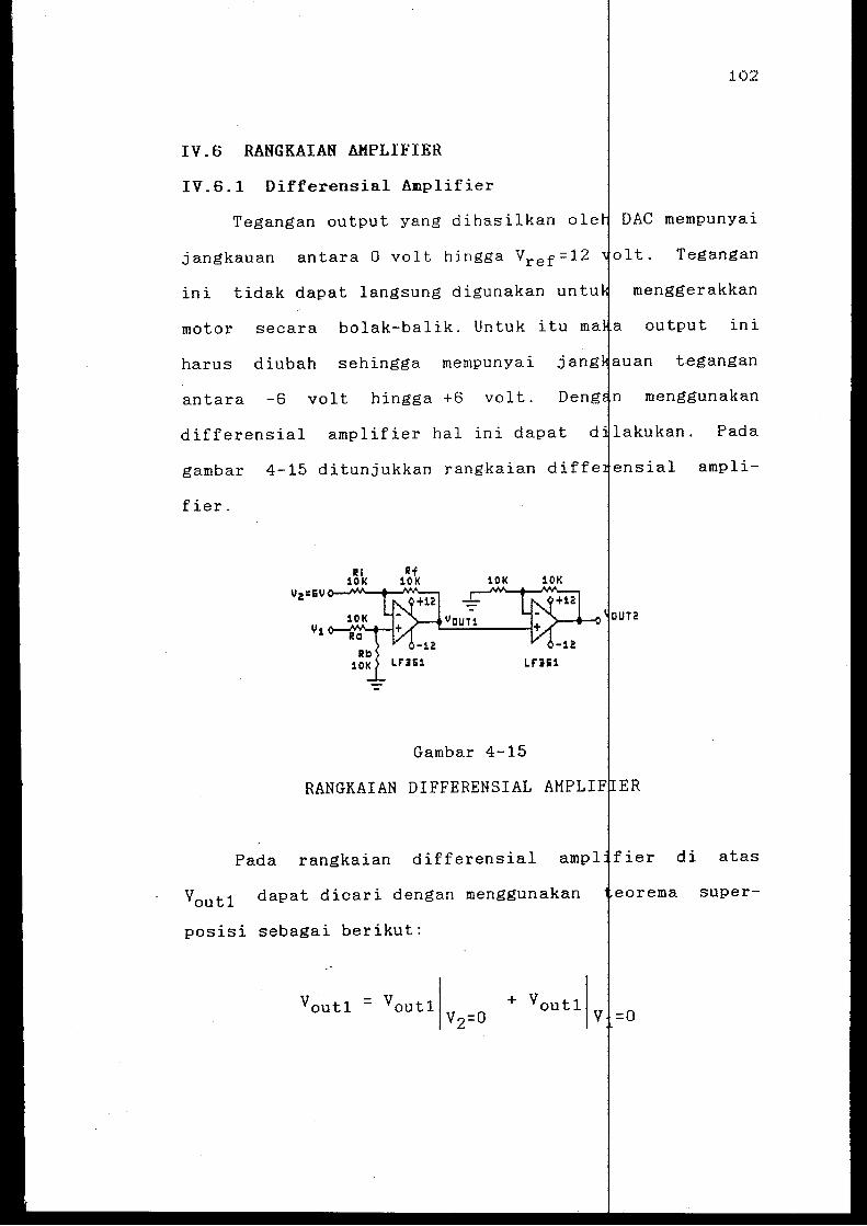
102
IV.6 RANGKAIAN AMPLIFIER
IV.6.1 Differensial Amplifier
Tegangan output yang dihasilkan ole DAC mempunyai
jangkauan antara 0 volt hingga Vref=12 olt. Tegangan
ini tidak dapat langsung digunakan untu menggerakkan
motor secara bolak-balik. Untuk itu ma a output ini
harus diubah sehingga mempunyai jang tegangan
antara -6 volt hingga +6 volt.
differensial amplifier hal ini dapat d lakukan. Pada
gambar 4-15 ditunjukkan rangkaian diffe
fier.
Rf 101< 101<
Gambar 4-15
10K
DUT2 I
RANGKAIAN DIFFERENSIAL AMPLI ER
ampli-
Pada rangkaian differensial ampl fier di atas
V0ut1 dapat dicari dengan menggunakan
posisi sebagai berikut:
Voutl = voutl Vz=O
+ voutl
eorema super-
v =0
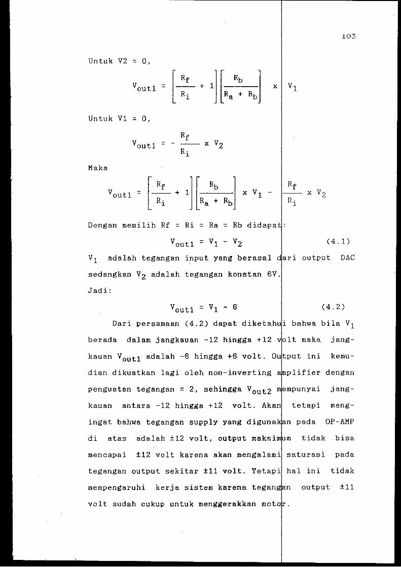
Untuk V2 = 0,
Untuk V1 = 0,
x v2
Maka
Dengan memilih Rf = Ri = Ra = Rb didapa
v2
v1 adalah tegangan input yang berasal
sedangkan v 2 adalah tegangan konstan 6V.
Jadi:
Dari persamaan (4.2) dapat
berada dalam jangkauan -12 hingga +12
kauan vout1 adalah -6 hingga +6 volt. 0
dian dikuatkan lagi oleh non-inverting
penguatan tegangan = 2, sehingga V0 ut2
kauan antara -12 hingga +12 volt. A
ingat bahwa tegangan supply yang digun
di atas adalah ±12 volt, output maksi
mencapai ±12 volt karena akan mengalam
tegangan output sekitar ±11 volt.
mempengaruhi kerja sistem karena
volt sudah cukup untuk menggerakkan mot
x v2
(4.1)
ri output DAC
(4.2)
bahwa bila v1
lt maka jang-
kemu-
lifier dengan
jang-
tetapi meng-
OP-AMP
tidak bisa
pad a
tidak
output ±11
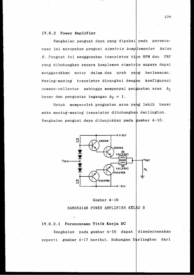
104
IV.6.2 Power Amplifier
Rangkaian penguat daya yang dipakai pada perenca-
naan ini merupakan penguat simetris k kelas
B. Penguat ini menggunakan transistor e NPN dan PNP
yang dihubungkan secara komplemen simetr s supaya dapat
menggerakkan motor dalam dua arah
Masing-masing transistor dirangkai deng
common-collector sehingga mempunyai
besar dan penguatan tegangan Av ~ 1.
Untuk memperoleh penguatan arus
maka masing-masing transistor dihubungk
Rangkaian penguat daya ditunjukkan pada
1!1 11<
u 11<
Gambar 4-16
berlawanan.
konfigurasi
besar
darlington.
ar 4-16.
RANGKAIAN POWER AMPLIFIER KEL S B
IV.6.2.1 Perencanaan Titik Kerja DC
Rangkaian pada gambar 4-16 dapat disederhanakan
seperti gambar 4-17 berikut. Hubungan D lington dari
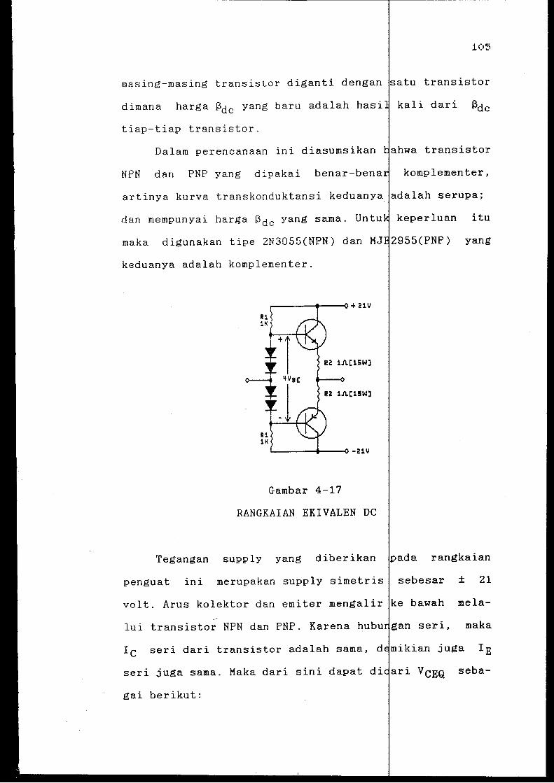
105
masing-masing transistor diganti dengan atu transistor
dimana harga ~de yang baru adalah hasi kali dari ~de
tiap-tiap transistor.
Dalam pereneanaan ini diasumsikan ahwa transistor
NPN dan PNP yang dipakai benar-bena komplementer,
artinya kurva transkonduktansi keduanya adalah serupa;
dan mempunyai harga ~de yang sama. Untu keperluan itu
maka digunakan tipe 2N3055(NPN) dan MJ 2955(PNP) yang
keduanya adalah komplementer.
+ uv
, ·r Rc 1.fl.[15WJ ~ "" RC 1.fl.(15WJ lj
111 1K
-uv
Gambar 4-17
RANGKAIAN EKIVALEN DC
Tegangan supply yang diberikan pada rangkaian
penguat ini merupakan supply simetris sebesar ± 21
volt. Arus kolektor dan emiter mengalir ke bawah mela-
lui transistor NPN dan PNP. Karena hubu gan seri, maka
Ic seri dari transistor adalah sama, d mikian juga IE
seri juga sama. Maka dari sini dapat di seba-
gai berikut:
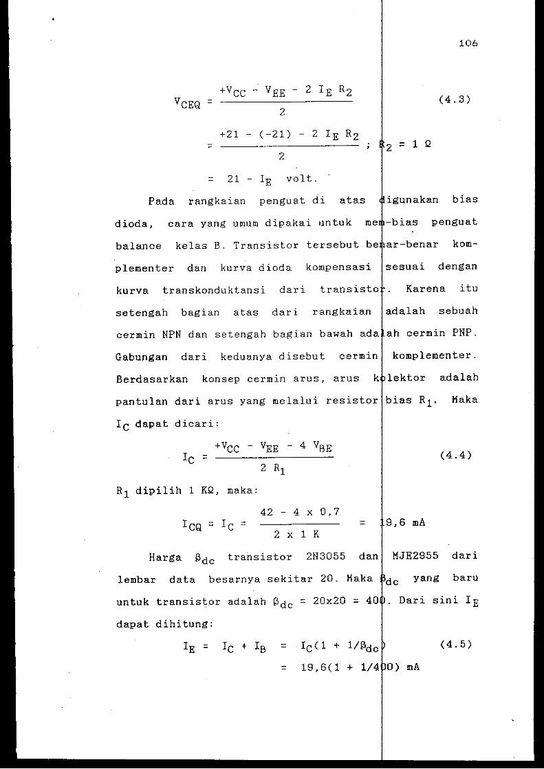
106
+Vee - VEE - 2 IE R2 VeEQ --
2 (4.3)
+21 - (-21) - 2 IE R2 = 2 = 1 Q
2
= 21 - IE volt.
Pad a rangkaian penguat di at as igunakan bias
dioda, cara yang umum dipakai untuk me -bias penguat
balance kelas B. Transistor tersebut be ar-benar kom-
plementer dan kurva dioda kompensasi sesuai dengan
kurva transkonduktansi dari transisto Karena itu
setengah bagian atas dari rangkaian adalah sebuah
cermin NPN dan setengah bagian bawah ada ah cermin PNP.
Gabungan dari keduanya disebut cermin komplementer.
Berdasarkan konsep cermin arus, arus k lektor adalah
pantulan dari arus yang melalui resistor bias R1. Maka
Ic dapat dicari:
Ie = +Vee - VEE - 4 VBE
2 R1
R1 dipilih 1 KQ, maka:
42- 4 X 0,7 IeQ = Ie =
2 X 1 K
(4.4)
= 9,6 mA
Harga ~de transistor 2N3055 dan MJE2955 dari
lembar data besarnya sekitar 20. Maka c yang baru
untuk transistor adalah ~de = 20x20 = 40 . Dari sini IE
dapat dihitung:
IE = Ie + Is = Ie ( 1 + 1/13dc (4.5)
= 19,6(1 + 1/4 0) mA
107
19,649 ~ 19 65 mA.
Oleh karena IE << 21, maka VcEQ ~ 21 vo t.
IV.6.2.2 Analisa AC
- Impedansi Input
-
-
Impedansi input sinyal besar d ri transistor
adalah:
z = nctc<RL + Re') in( basis) ~>' (4.6)
dengan R1 = resistansi beban.
Re'= resistansi ac dioda emiter.
Dari hasil pengukuran didapat r sistansi beban
(motor) R1 = 10 Q. Sedangkan Re' d. eroleh melalui
rumus berikut:
Re' = 25 mV I IE ( 4. 7)
Maka:
eenguatan
eenguatan
= 25 mV I 19,6 mA
= 1,27 Q.
zin(basis) = 400(10 + 1, 7) = 4508
= 4,5 KQ
tegangan RL
Av = RL + R ,
e
10 =
10 + 1,27
= 0,88
DaY a RL
~ = 1:3ctc RL + Re
,
= 400 X 0,88
= 352
(4.8)
(4.9)
- Day a Out12ut Maksimum
Po( max) VeEQ Ie<
= 2
Sedangkan: Ie(sat) = VeEQIRL
Jadi: VeEQz po(max) =
2 RL
= 22,05
Dari lembar data, daya output maks
bolehkan untuk transistor 2N3055
40 watt, jadi daya output dari ran
masih berada dalam jangkauan yang
memenuhi syarat untuk digunakan.
108
t) (4.10)
2F
2 X 10
m yang diper-
adalah
di atas
dan
- Efisiensi DaYa Maksimum
Efisiensi daya adalah rasio ant
dengan daya input de, atau n = P 0 /P
daya output
Disipasi daya untuk rangkaian pen at kelas B di
atas adalah:
Poe = <Vee-VEE noe
dengan Ioe adalah arus pada transist
(4.11)
dirata-
rata dalam satu cycle. Karena arus yang mengalir
pada transistor merupakan sinyal set gah gelombang
untuk masing-masing. bagian (bagian
PNP), maka:
1oc =
=
1e(sat)
Tt
N dan bagian
(4.12)
109
21 =
Tt X 10
= 0,67 A.
Persamaan (4.11) didapat:
Poe = 42 v x o,67 A= 28,14
Jadi: 22,05
n = ~ 0,78 6 28,14
= 78,36 %
III.7 MOTOR
Motor yang dipergunakan adalah
medan magnet tetap. Seperti telah d
pengaturan kecepatan motor dapat
mengubah-ubah tegangan jangkar yang
tegangan sumber yang dikenakan pada
yang dibutuhkan motor adalah ±12 Volt
ampere, cukup kuat untuk menggerakkan
terlalu berat karena pada badan motor
gigi untuk memperbesar torsi motor.
IV.8 PERENCANAAN PERANGKAT LUNAK (
Pada perencanaan perangkat
bagian yang akan dibahas yaitu mengenai
data dari komputer IBM PC/XT ke memori
kontroler dan sekaligus mencek
Kedua adalah mengenai proses
sistem kontroler.
DC dengan
bahwa
ukan dengan
mengatur
Tegangan
gan arus ±1
tidak
terdapat roda
ini ada dua
transfer
sistem
datanya.
motor oleh
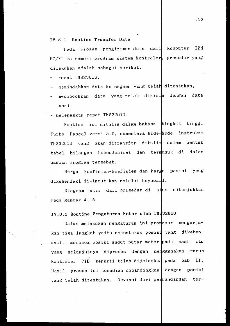
110
IV.8.1 Routine Transfer Data
Pada proses pengiriman data dar· komputer IBM
PC/XT ke memori program sistem kontroler prosedur yang
dilakukan adalah sebagai berikut:
reset TMS23010,
memindahkan data ke segmen yang tela
mencocokkan data yang telah dikir
asal,
- melepaskan reset TMS32010.
Routine ini ditulis dalam bahasa
ditentukan,
dengan data
ingkat tinggi
Turbo Pascal versi 5.0, sementara kode ode instruksi
TMS32010 yang akan ditransfer
tabel bilangan heksadesimal dan
bagian program tersebut.
Harga koefisien-koefisien
dikehendaki di-input-kan melalui keybo
Diagram alir dari prosedur di
pada gambar 4-18.
IV.8.2 Routine Pengaturan Motor
Dalam melakukan pengaturan
kan tiga langkah yaitu menentukan
daki, membaca posisi sudut putar
yang selanjutnya diproses dengan
kontroler PID seperti telah dijelask
Hasil proses ini kemudian dibandingkan
dalam bentuk
suk di dalam
posisi yang
ditunjukkan
2010
sor mengerja
yang dikehen
ada saat itu
rumus
bab II.
posisi
yang telah ditentukan. Deviasi dari pe andingan ter-
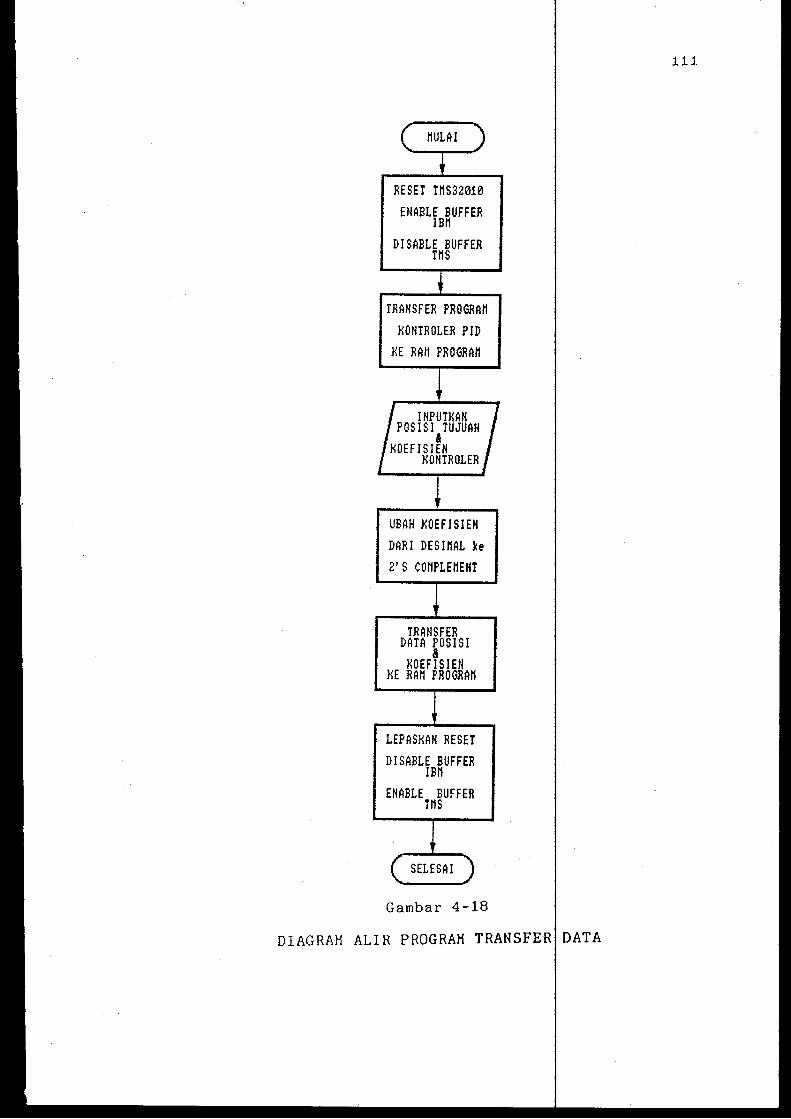
RESET TMS32010 ENABLE BUFFER
IBM DISABLE BUFfER
TMS
TRANSFER PROGRAM XONTROLER PID
XE RAM PROGRAM
UBAH XOEFISIEH DARI DESIMAL ke
2'S COMPLEMENT
TRANSFER DATA POSISI
& XOEFISJEN
XE RAM PROGRAM
LEPASXAH RESET DISABLE BUFFER
IBM ENABLE BUFFER
TMS
Gambar 4-18
DIAGRAM ALIR PROGRAM TRANSFER DATA
111
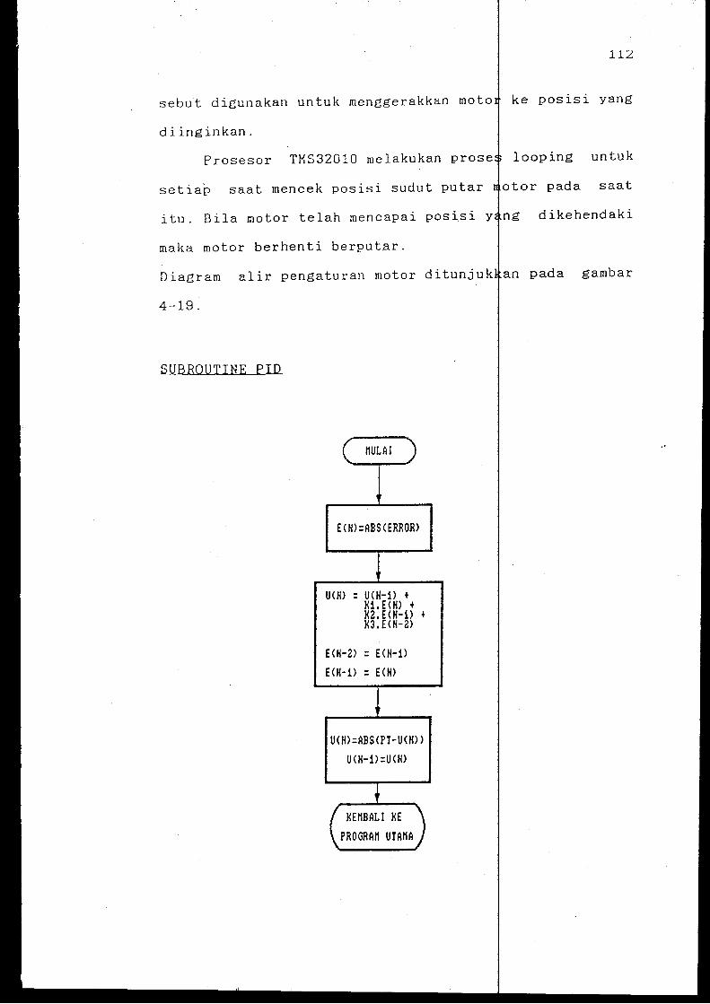
112
sebut digunakan untuk menggerakkan moto ke posisi yang
diinginkan.
Prosesor TMS32010 melakukan prose looping untuk
setiap saat mencek posisi sudut putar otor pada saat
itu. Bila motor telah mencapai posisi y ng dikehendaki
maka motor berhenti berputar.
Diagram alir pengaturan motor ditunjuk an pada gambar
4-19.
SUBROUTINE PID
E<H>=ABS<ERROR>
U<H> = U<H-1> + Hi.E(H) + H2.E<H-1> + H3.E<H-2>
E<H-2> = E<H-1) E<H-1> = E<H>
U<H>=ABS<PT-U<H>> U<H-1>=U<H>
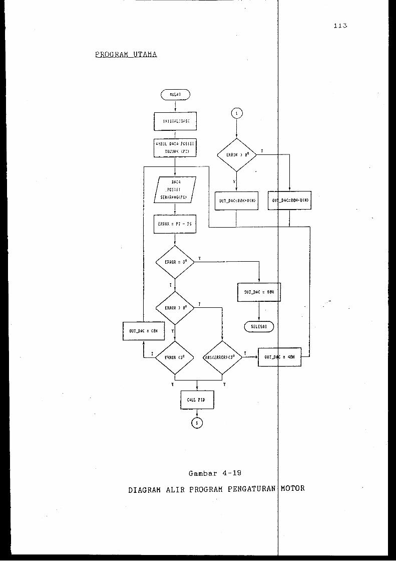
PROGRAM UTAMA
( nuL~! )
lNISi~L!S;.SI
Gambar 4-19
DIAGRAM ALIR PROGRAM PENGATURAN MOTOR
I
V.l PENDAHULUAN
BAB V
PENGUJIAN ALAT
Pacta bab ini akan diberikan hasil engujian alat
yang telah dibuat berdasarkan perencan pad a Bab IV.
Pengujian dibagi menjadi tiga bagian ber asarkan blok
blok yang diukur, yaitu pengujian pacta:
1. Modul Kontroler, mengenai pengukuran pacta Prosesor
TMS32010 yang meliputi clock output ( LKOUT), strobe
MEN, WE dan DEN.
2. Modul Sensor, meliputi pengukuran c ok ADC 0804,
sinyal output interrupt INTR dan asil konversi
posisi derajat ke data biner.
3. Modul Aktuator, meliputi pengukuran 'asil konversi
data biner ke tegangan analog, outpu Differensial
Amplifier, output Power Amplifier an ketelitian
posisi derajat.
Adapun bentuk fisik alat tersebut d tunjukkan pacta
gambar 5-1.
V.2 PENGUJIAN MODUL KONTROLER
Prosesor TMS32010 bekerja dengan
dengan frekuensi kristal 10 MHz. Sesuai
kerja clock ~pternal pacta TMS32010,
pacta pin CLKOUT adalah 1/4 frekuensi
fc = 2,5 MHz. Hasil pengukuran dapat
gambar 5-2.
114
lock internal
engan prinsip
kuensi output
kristal, j ad i
dilihat pada
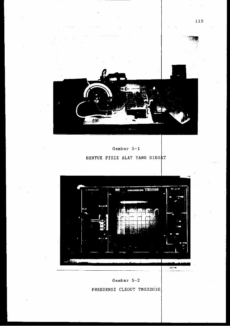
115
Gambar 5-1
BENTUK FISIK ALAT YANG
Gambar 5-2
FREKUENSI CLKOUT THS32010
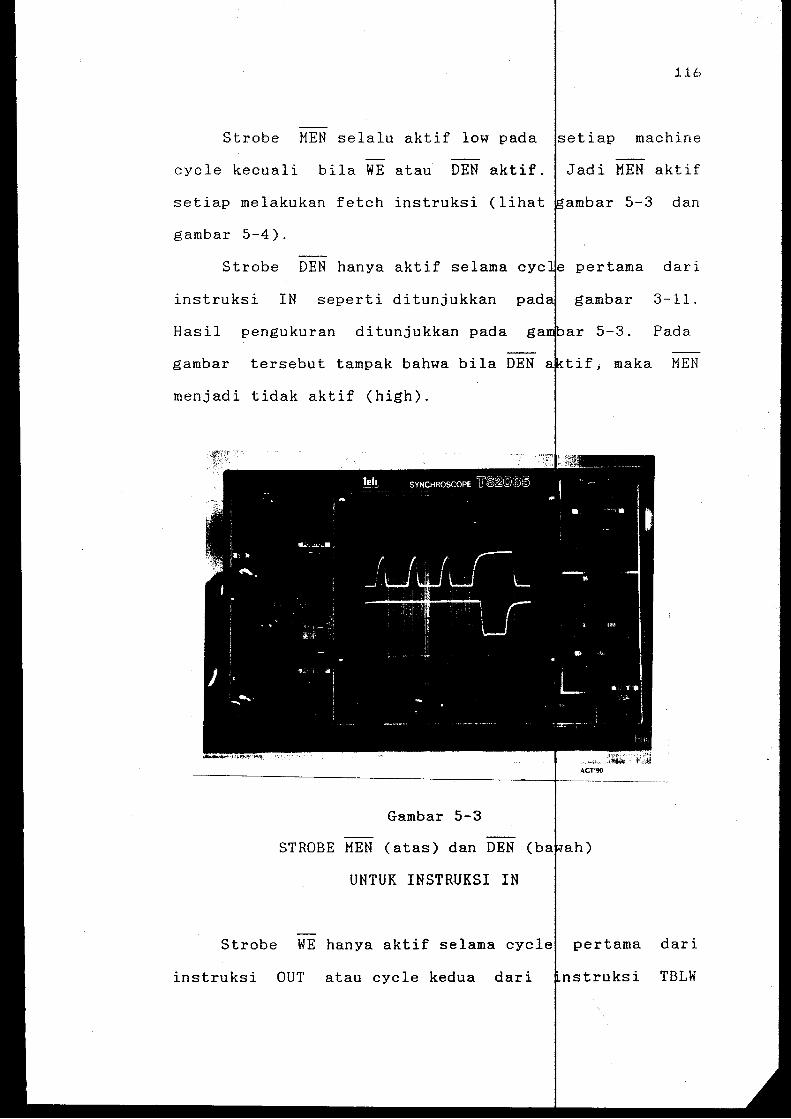
116
Strobe MEN selalu aktif low pada etiap machine
cycle kecuali bila WE atau DEN aktif. Jadi MEN aktif
setiap melakukan fetch instruksi
gambar 5-4).
Strobe DEN hanya aktif selama
instruksi IN seperti ditunjukkan
Hasil pengukuran ditunjukkan pada g
gambar tersebut tampak bahwa bila DEN
menjadi tidak aktif (high).
Gambar 5-3
ambar 5-3 dan
pertama dari
gambar 3-11.
ar 5-3. Pada
tif, maka MEN
STROBE MEN (atas) dan DEN (b ah)
UNTUK INSTRUKSI IN
Strobe WE hanya aktif selama cycle pertama dari
instruksi OUT atau cycle kedua dari .nstruksi TBLW
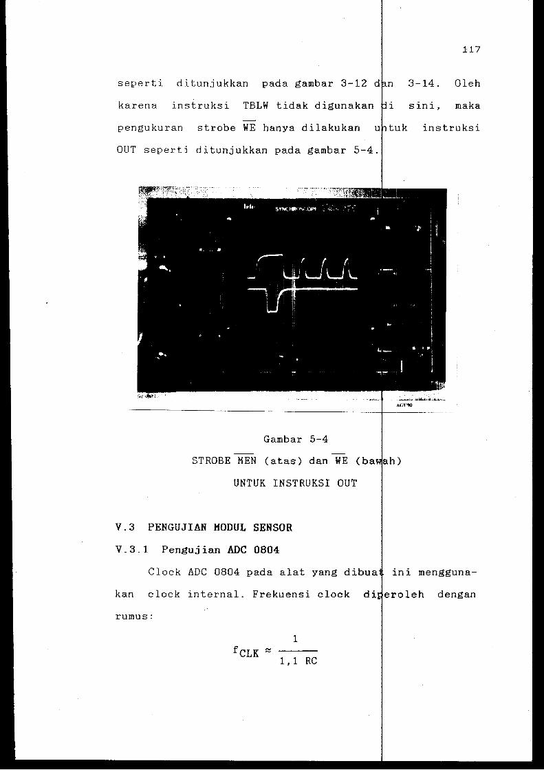
117
seperti ditunjukkan pada gambar 3-12 d n 3-14. Oleh
karena instruksi TBLW tidak digunakan i sini, maka
pengukuran strobe WE hanya dilakukan
OUT seperti ditunjukkan pada gambar 5-4.
Gambar 5-4
AGT'90
STROBE MEN (atas) dan WE (b h)
UNTUK INSTRUKSI OUT
V.3 PENGUJIAN MODUL SENSOR
V.3.1 Pengujian ADC 0804
instruksi
Clock ADC 0804 pada alat yang dibua ini mengguna
kan clock internal. Frekuensi clock d eroleh dengan
rumus:
1 fcLK ~
1,1 RC
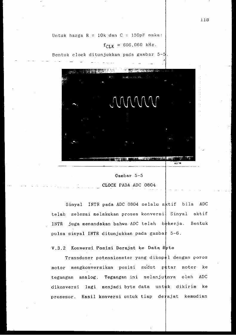
Untuk harga R = lOk dan C = 150pF maka:
fcLK z 606,060 kHz.
Bentuk clock ditunjukkan pada gambar
Gambar 5-5
CLOCK PADA ADC 0804
118
Sinyal INTR pada ADC 0804 tif bila ADC
telah selesai melakukan proses konversi Sinyal aktif
INTR juga menandakan bahwa ADC telah b kerja. Bentuk
pulsa sinyal INTR ditunjukkan pada gamba 5-6.
V.3.2 Konversi Posisi Derajat ke Data te
Transduser potensiometer yang dikop l dengan poros
motor mengkonversikan posisi sudut p tar motor ke
tegangan analog. Tegangan ini selanju nya oleh ADC
dikonversi lagi menjadi byte data unt k dikirim ke
prosesor. Hasil konversi untuk tiap de ajat kemudian
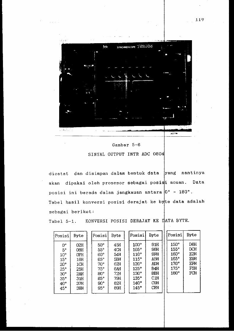
119
Gambar 5-6
SINYAL OUTPUT INTR ADC 080
dicatat dan disimpan dalam bentuk data nantinya
akan dipakai oleh prosesor sebagai posi acuan. Data
posisi ini berada dalam jangkauan antara - 180°.
Tabel hasil konversi posisi derajat ke b e data adalah
sebagai berikut:
Tabel 5-1. KONVERSI POSISI DERAJAT KE
Posisi Byte Posisi Byte Posisi Byte Posisi Byte
oo 02H 50° 45H 100° 91H 150° D6H so 08H 55° 4CH 105° 98H 155° DCH
100 OFH 60° 54H 110° 9FH 160° E2H 15° 16H 65° 5BH 115° ASH 165° E9H 20° 1CH 70° 62H 120° ADH 170° EFH 25° 25H 75° 6AH 125° B4H 175° F5H 30° 2AH goo 72H 130° BBH 180° FCH 35° 31H 85° 79H 135° ClH 40° 37H goo 82H 140° C9H 45° 3EH 95° 89H 145° CFH
120
V.4 KODUL AKTUATOR
V.4.1 Pengujian DAC 0808
DAC 0808 pada alat yang dibua menggunakan
tegangan referensi +12 volt. Tegangan ou put DAC dapat
dihitung dari rumus:
Az --+
4 ... +
Al Az = 12V (-- + + ... +
2 4
dengan A1 MSB dan As LSB.
Hasil pengukuran untuk beberapa sampel
Tabel 5-2. HASIL KONVERSI DAC
vo Input Byte Data Perhitungan
(V)
00 0,00 10 0,75 20 1,50 30 2,25 40 3,00 50 3,75 60 4,50 70 5,25 80 6,00 90 6,75 AO 7,50 BO S,25 co 9,00 DO 9,75 EO 10,50 FO 11,25
V.4.2 Pengujian Differensial Amplifier
i
p
I
As +--)
256
As )
256
put adalah:
vo ngukuran
(V)
0,006 0,74S 1,499 2,240 2,990 3,730 4,4SO 5,220 5,980 6,720 7,470 8,210 S,960 9,700 0,450 1,060
Differensial Amplifier berfungsi un uk menurunkan
level tegangan output dari DAC yang bera a dalam jang-
121
kauan antara 0 hingga Vmaks menjadi - /2Vmaks hingga
+1/2Vmaks· Ini dimaksudkan agar dap t menggerakkan
motor dalam dua arah.
Berdasarkan persamaan (4.2) maka egangan output
differensial amplifier adalah:
vo(Diff) = vo(DAC) - 6
Hasil pengukuran untuk beberapa sampel nput ditunjuk-
kan pada tabel 5-3.
Tabel 5-3. PENGUKURAN DIFFERENSIAL AM LIFIER
Input Vo(DAC) Vo(Diff) o(Daff) Byte Perhitungan ngu uran Data (V) (V) (V)
00 0,006 -5,994 -5,840 10 0,748 -5,252 -5,090 20 1,499 -4,501 -4,330 30 2,240 -3,760 -3,590 40 2,990 -3,010 -2,830 50 3,730 -2,270 -2,090 60 4,480 -1,520 -1,330 70 5,220 -0,780 -0,594 80 5,980 -0,020 0,174 90 6,720 0,720 0,918 AO 7,470 1,470 1,673 BO 8,210 2,210 2,410 co 8,960 2,960 3,170 DO 9,700 3,700 3,910 EO 10,450 4,700 4,660 FO 11,060 5,060 5,270
V.4.3 Pengujian Power Amplifier
Output differensial amplifier yang mempunyai level
tegangan -1/2Vmaks hingga +1/2Vmaks kem ian diperkuat
oleh non-inverting amplifier sehingga level tegangan
output menjadi -Vmaks hingga +Vmaks· Level tegangan
tersebut kemudian diumpankan ke power a lifier. Hasil
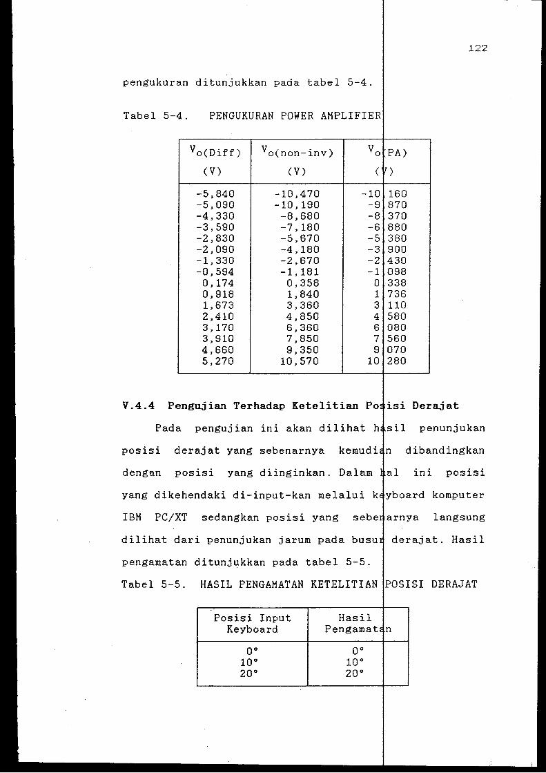
122
pengukuran ditunjukkan pada tabel 5-4.
I
Tabel 5-4. PENGUKURAN POWER AMPLIFIER I
Vo(Diff) vo(non-inv) vo PA)
(V) (V) ( )
!
-5,840 -10,470 -10 ! 160 -5,090 -10,190 -9 1870 -4,330 -8,680 -8 370 -3,590 -7,180 -6 880 -2,830 -5,670 -5 i380 -2,090 -4,180 -3 900 -1,330 -2,670 -2 430 -0,594 -1,181 -1 098 0,174 0,358 0 338 0,918 1,840 1 736 1,673 3,360 3 110 2,410 4,850 4 580 3,170 6,360 6 080 3,910 7,850 7 560 4,660 9,350 9 070 5,270 10,570 10 280
V.4.4 Pengujian Terhadap Ketelitian Po isi Derajat
Pacta pengujian ini akan dilihat h sil penunjukan
posisi derajat yang sebenarnya kemudi n dibandingkan
dengan posisi yang diinginkan. Dalam al ini posisi
yang dikehendaki di-input-kan melalui yboard komputer
IBM PC/XT sedangkan posisi yang seb arnya langsung
dilihat dari penunjukan jarum pada derajat. Hasil
pengamatan ditunjukkan pada tabel 5-5.
Tabel 5-5. HASIL PENGAMATAN KETELITIAN POSISI DERAJAT
Posisi Input Keyboard
Hasil Pengamat
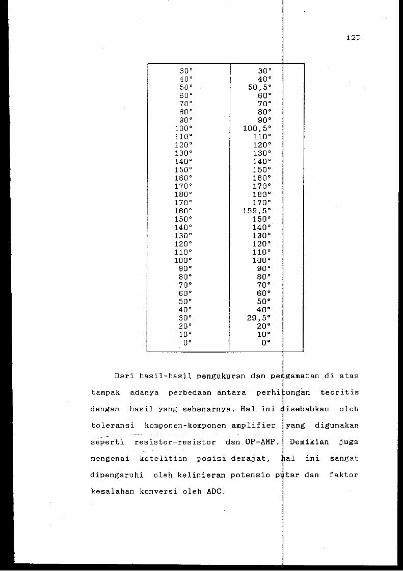
123
30° 30° 40° 40° 50° 50,5° 60° 60° 70° 70° 80° 80° goo goo
100° 100,5° 110° 110° 120° 120° 130° 130° 140° 140° 150° 150° 160° 160° 170° 170° 180° 180° 170° 170° 160° 15g,5o 150° 150° 140° 140° 130° 130° 120° 120° 110° 110° 100° 100°
goo goo 80° 80° 70° 70° 60° 60° 50° 50° 40° 40° 30° 2g,5o 20° 20° 10° 10°
oo oo
Dari hasil-hasil pengukuran dan p gamatan di atas
tampak adanya perbedaan antara ungan teoritis
dengan hasil yang sebenarnya. Hal ini isebabkan oleh
toleransi komponen-komponen amplifier yang digunakan
seperti resistor-resistor dan OP-AMP. Demikian juga
mengenai ketelitian posisi derajat, al ini sangat
dipengaruhi oleh kelinieran potensio p tar dan faktor
kesalahan konversi oleh ADC.

BAB VI
KESIMPULAN
Dari keseluruhan perencanaan dan embuatan alat
dapat diambil beberapa kesimpulan sebag i berikut:
1. Kontroler PID digital merupakan
gunaan kontroler PID analog
unggulan yang dimiliki antara lain:
parameter-parameternya tidak
faktor luar seperti lama pemakaian
temperatur ruang.
mempunyai fleksibilitas tinggi
dapat diubah-ubah secara software.
2. Pada pengaturan posisi dengan kontro
ketelitian derajat putaran ditentu
ADC dan kelinieran pada
dipakai. Dengan menggunakan ADC
resolusi 8 bit, secara ideal akan
putaran motor hingga 256° bila seti
representasikan dengan 1 bit. Akan
juga ditentukan oleh kelinieran
sebagai transduser posisi. Bila d
resolusi yang lebih besar
mampu mendeteksi sebanyak
pada masalah keterbatasan transduser
yang tidak bisa berputar lebih
keperluan tersebut maka rancangan
dimodifikasi yaitu transduser patens
124
peng
beberapa ke-
oleh
faktor
koefisien
digital,
resolusi
posisi yang
mempunyai
u mendeteksi
derajat di
hal ini
putar
an ADC dengan
akan
kembali lagi
putar
360°. Untuk
perlu
tidak dikopel
125
langsung ke poros motor, melainkan m alui roda gigi
transmisi dengan perbandingan diamet r yang sesuai.
3. Penggunaan Prosesor Sinyal Digital TMS32010 yang
memiliki kecepatan eksekusi yang cuk
gai pemroses dalam operasi aritmat
implementasikan algoritma kontroler
diperoleh ouput yang real-time.
4. Sistem kontroler ini juga dapat
pengaturan posisi menggunakan motor
ubah modul aktuator dan menyesuaik
Selain itu alat 1n1 juga bisa
untuk pengaturan kecepatan motor
dengan mengubah modul sensor dan/at
tinggi seba
untuk meng
digital akan
nakan untuk
dengan meng
softwarenya.
k DC maupun AC
bAfTAJt PU.S
•

DAFTAR PUSTAKA
1. Borland, Bor-
land International
2. Carr, Joseph J.,
tat ion and H easuremen t, Company,
Inc. , 1979.
3. Coughlin, Robert F., Frederick F. Dr scoll, Ooera-
Prentice-Hall Inc.,
4. Eggebrecht. Lewis C.,
ComPLl ter. Howard
5. Gopal, H.,
Eastern Limited,
6. Hall, Douglas V.,
McGraw-Hill Book Co., Singapore,
7. Kaiser, Joe., Electrical Power.
Company, Inc. (illinois),1982.
8. Maloney, Timothy J.,
tronics, Prentice-Hall,
9. Malvino, Albert Paul.,
MCGraw-Hill Inc., 1979.
10. Ogata, Katsuhiko.,
11. Quarmby, David J.,
Publishing Ltd., London, 1984.
12. Sumarto, Drs., Hesin A·rus Searab,
karta,1984.
126
Wiley
New
Granada
127
National 13. . ...... '
14. Texas
Instruments Inc. ,1988.
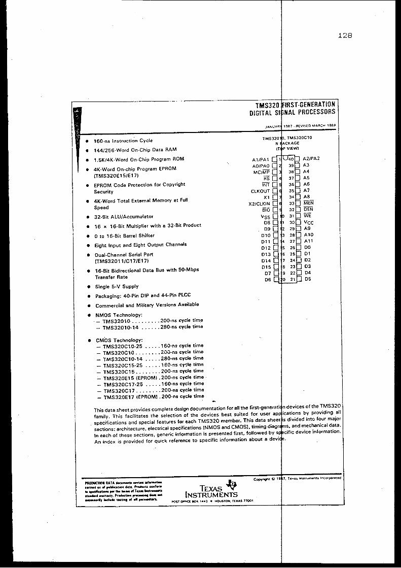
• 160-ns Instruction Cycle
e 144/256-Word On-Chip Data RAM
• 1.5K/4K-Word On-Chip Program ROM
• 4K-Word On-chip Program EPROM (TMS320E15/E171
• EPROM Code Protection for Copyright Security
• 4K-Word Total External Memory at full Speed
• 32-Bit ALU/Accumulator
• 16 x 16-Bit Multiplier with a 32-Bit Product
• 0 to 1 6-Bit Barrel Shifter
• Eight Input and Eight Output Channels
• Dual-Channel Serial Port (TMS32011/C17/E171
• 16-Bit Bidirectional Data Bus with 50-Mbps Transfer Rate
• Single 5-V Supply
• Packaging: 40-Pin DIP and 44-Pin PLCC
• Commercial and Military Versions Available
• NMOS Technology: - TMS3201 0 .......•. 200-ns cycle time - TMS32010-14 ...... 280-ns cycle time
• CMOS Technology: - TMS320C10-25 •..•. 160-ns cycle time - TMS320C10 ........ :200-ns cycle time - TMS320C1 0-14 ..... 280-ns cycle time - TMS320C 15-25 ..... 160-ns cy-;le tima - TMS320C15 ........ 200-ns cycle time - TMS320E 15 (EPROM! . 200-ns cycle time - TMS320C17-25 ..•.• 160-ns cycls time - TMS320C1 7 ........ 200-ns cycle time - TMS320E17 (EPROM! . 200-ns cycle time
Al/PAl
ST-GENERATION L PROCESSORS
A2/PA2
A3 A4 A5 A6 A7 AS MEN DEN WE
Vee A9 AlO All
DO 01
D2 03 04
-;..L:.._:...:.r-- D5
128
This data sheet provides complete design documentation for all the fi"''·'""'""'"'rlln family. This facilitates the selection of the devices best suited for user applu:at1or1s by providing all specifications and special features for each TMS320 member. This data sheet divided into four major sections: architecture, electrical specifications (NMOS and CMOS), timing and mechanical data. In each of these sections, generic information is presented first, followed An index is provided for quick reference to specific information about a
I'ROOUCliO& DATA lloao---,.,. .. , .... ,.Wic.at ... ...... Pt-'ecU c.e•f...-. ,.~,. ... -.tr .... -,..-...,...., __ ,._...._ ... __., - too11ot of oil ,.,_.,._
TEXAS -lj} INSTRUMENTS
POSt OHICI 80JI. 1Ul • HOUSTON. TEXAS 7700t
DEVICES
description
The TMS320 family of 16/32-bit single-chip digital signal processors combines speed controller with the numerical capability of an array processor, thereby alternative to multichip bit-slice processors. The highly paralleled architecture and provide speed and flexibility to produce aMOS microprocessor family capable of ex<AcLn•n•a
instructions per second). The TMS320 family optimizes speed by imol••mentino "'"'"'..,'""' other processors implement through microcode or software. This hard...,,.,.,,_;r,tAn<,iviR the design engineer with processing power previously unavailable on a single
The TMS320 family consists of two generations of digital signal processors. The the TMS32010 and its spinoffs, as described in this data sheet. The TMS32020 the second-generation processors, designed fornigher performance. Many """""'''"""' common among the TMS320 processors. Specific features are added in each processor to provide cost/performance tradeoffs. Software compatibility is maintained throughout the family to protect user's investment in architecture. Each processor has software and hardware tools to facilitate design.
introduction
The TMS32010, the first NMOS digital signal processor in the TMS320 family, Its powerful instruction set. inherent flexibility. high-speed number-crunching ,.~n~hlr::.;.,~ architecture have made this high-performance, cost-effective processor the telecommunications. computer, commercial, industrial, and military applications. TMS320C10, a low-power CMOS version of the industry-standard TMS32010, and have been added to the first generation of the TMS320 family.
The TMS3201 0 microprocessor is available in two speed versions: TMS3201 0 (20 l 14 MHzi. These devices are capabie of executing a 16 x 16-bit multiply with a instruction cycle. On-chip data RAM of 144 words and on-chip program ROM of 1 Full-speed execution of 4K words of off-chip program memory is also possible. The a low-cost alternative for DSP applications not requiring the maximum nn<> .. •ti~•n TMS32010. The device provides a direct EPROM interface for cost-effective modification. Both of these devices are pin-for-pin and object-code compatible
result in a single are available.
10-14 provides frequency of the development and
the TMS3201 0 and
its development tools.
The TMS320C10 is object-code and pin-for-pin compatible with the TMS32010.1t processed in CMOS technology. achieving a power dissipation less than one-sixth that of the NMOS The lower power dissipation makes the TMS320C10 ideal for power-sensitive applications such telephony and portable P'oducts. The TMS320C 10-25, a 25-MHz version of the TMS320C1 0, 160-ns instruction cycle time and is well suited for high-performance OSP applications. The TM 10 is also available in a 280-ns version, the TMS320C 1 0-14. This device provides a low-cost ~., .... ,~.: .. ~o for DSP applications
not requiring the maximum operating frequency of the TMS320C10.
The TMS320C 15 and TMS320E15 CMOS devices are object-code and nino-tn.r-n,irll TMS3201 0 and. offer expanded on-chip RAM of 2 56 words and on-chip words. These devices allow the capability of upgrading performance and and system cost without hardware redesign. The TMS320C 15 is also available in
TMS320C15-25.
TEXAS~ INSTRUMENTS
POST OHtC( &0A 1U] • t4()VSTON. T(XAS 77001
129
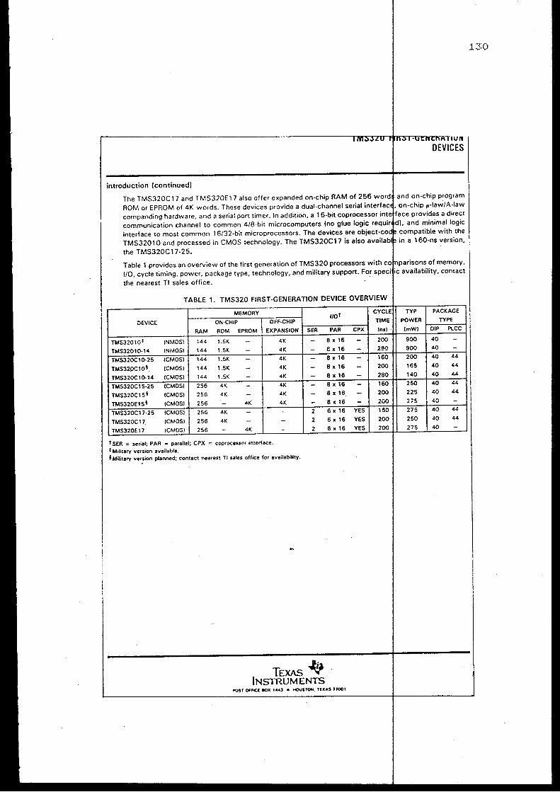
tun DEVICES
introduction (continued)
The TMS320C 17 and TMS320E 1 7 also offer expanded on-chip RAM of 256 word and on-chip program ROM or EPROM of 4K words. These devices provide a dual-channel serial on-chip ,.-law/A-law companding hardware. and a serial port timer. In addition, a 16-bit coprocessor ont""'~r·" provides a direct communication channel to common 4/8-bit microcomputers (no glue logic ). and minimal logic interface to most common 16/32-bit microprocessors. The devices are compatible with the TMS3201 0 and processed in CMOS technology. The TMS320C17 is also avail
the TMS320C17-25.
Table 1 provides an overview of the first generation of TMS320 processors with 1/0, cycle timing. power, package type, technology, and military support. For spe the nearest Tl sales office. ·
TABLE 1.
DEVICE
RAM ROM
TMS32010t !NMOS! 144 1.5K
!NMOS! 144 1.5K
tCMOSl 144 , .!>K
(CMOS! 144 1.5K
144 l.SK
255 4K
255 4K
tCMOSl 255 4K
tCMOSl 255 4K
TMS320C17 !CMOS! 256 4K
TMS320E1 7 !CMOS) 256 4K
t SER = serial; PAR = parallel: CPX = coprocessor interface. t Military version available.
4K
4K
4K
4K
4K
4K
I Military version planned: contact nearest TJ sates office for availability.
2
2
2
TEXAS~ INSTRUMENTS
8 X
8 X 16
8 X 16
6 X 16
6 X 16
6 X 16
POST ()f'ftCl .OX U.U e HOUSfON. TfXA$ UOOI
280
160
200
200
160
YES 200
YES 200
arisons of memory, availability, comact
PACKAGE
44
44
44
44
44
275 44
250 40 44
275 40
130
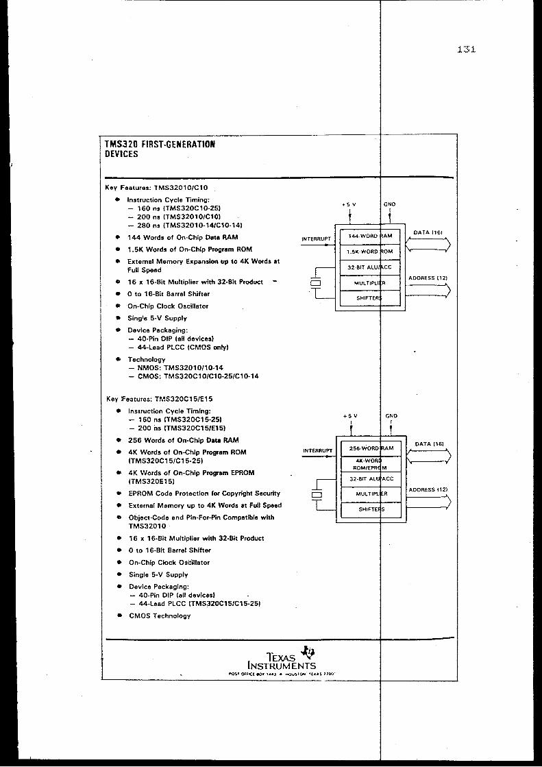
TMS320 FIRST-GENERATION DEVICES
Key Features: TMS32010/C10
• Instruction Cycle Timing: - 160 ns (TMS320C10·251 - 200 ns (TMS32010/C101 - 280 ns (TMS32010·14/C10·141
• 1 44 Words of On-Chip Data RAM
• 1.5K Words of On-Chip Program ROM
• External Memory Expansion up to 4K Words at full Speed
• 16 x 1 6-Bit Multiplier with 32-Bit Product
• 0 to 1 6-Bit Barrel Shifter
• On-Chip Clock Oscillator
• Sing'e 5-V Supply
• Device Packaging: - 40-Pin DIP (all devices) - 44-lead PLCC (CMOS on!y!
• Technology - NMOS: TMS32010/10·14 - CMOS: TMS320C10/Ct0-25/C10·14
Key Features: TMS320C1 5/E15
• Instruction Cycle Timing: - 160 ns (TMS320C15-251 - 200 ns (TMS320C1 5/Et51
• 256 Words of On-Chip Data RAM
• 4K Words of On-Chip Program ROM tTMS320C1 5/C1 5-251
• 4K Words of On-Chip Program EPROM !TMS320E1 51
• EPROM Code Protection for Copyright Security
• External Memory up to 4K Words at Full Speed
• Object-Code and Pin-For-Pin Compatible with TMS32010
• 16 x 1 6-Bit Multiplier with 32-Bit Product
• 0 to 1 6-Bit Barrel Shifter
• On-Chip Clock Osditlator
• Single 5-V Supply
• Device Packaging: - 40-Pin DIP (all devices) - 44-lead PLCC ITMS320C15/C15-251
• CMOS Technology
TEXAS lf} INSTRUMENTS
131
• 5 v GNO
+5 v GNO
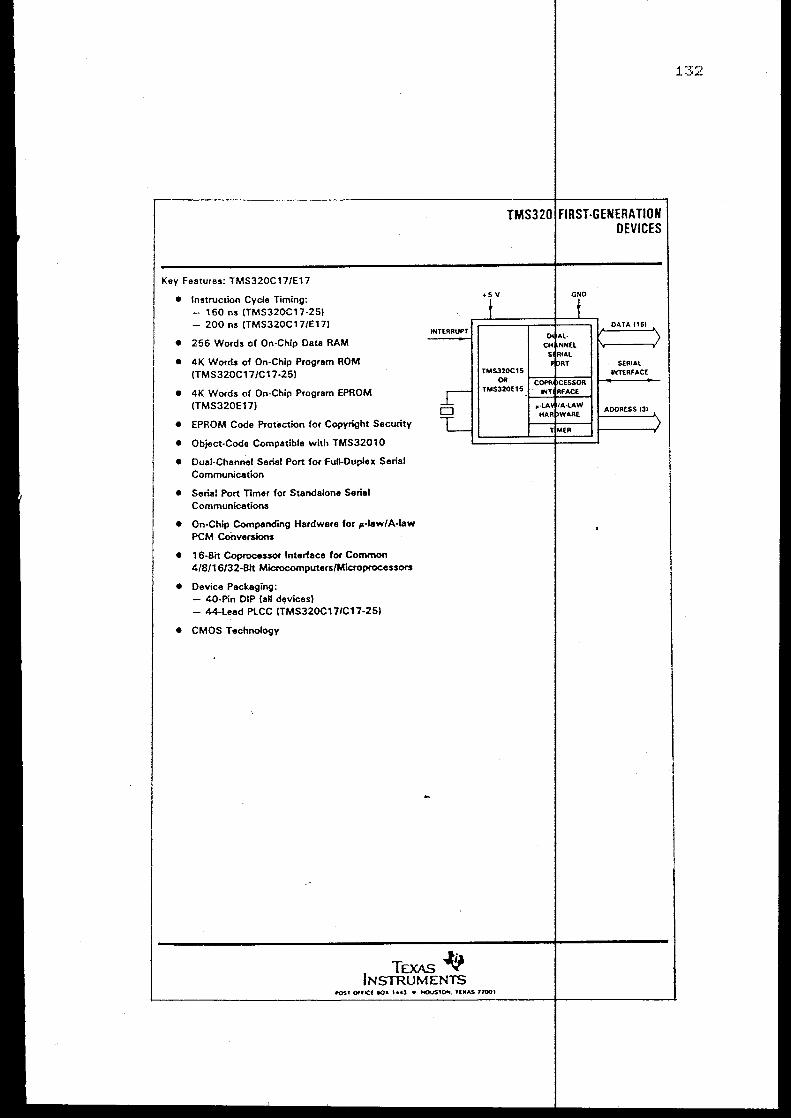
Key Features: TMS320C17/E17
• Instruction Cycle Timing: - 160 ns (TMS320C17-25) - 200 ns (TMS320C17/E17)
• 256 Words of On-Chip Data RAM
• 4K Words of On-Chip Program ROM ITMS320C17/C17-25)
• 4K Words of On-Chip Program EPROM (TMS320E17)
• EPROM Code Protection for Copyright Security
• Object-Code Compatible with TMS32010
• Dual-Channel Serial Port for Full-Duplex Serial Communication
• Serial Port Timer for Standalone Serial Communications
• On-Chip Compending Hardware for ,.-taw/A-law PCM Conversions
• 16-Bit Coproceuor Interface for Common 4/8/1 6/32-Bit Microcomputers/Microprocessors
• Device Packaging: - 40-Pin DIP (all devices) - 44-Lead PLCC ITMS320C17/C17-25)
e CMOS Technology
INT£RRUPT
TEXAS~ INSTRUMENTS
•5 v
lOSt OlfC( .01t 1441 • HQUSl()trrjl. f(Ut.S 17001
TMS320 FIRST-GENERATION DEVICES
GNO
DATA (161
SERIAl INTERFACE
AOORESS 131
132
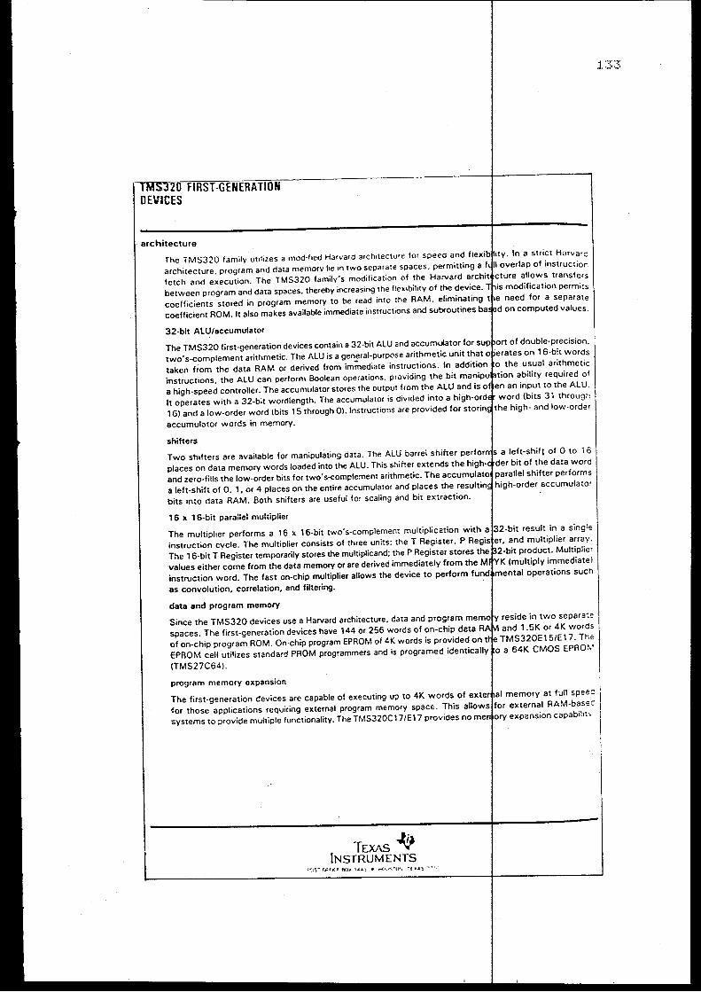
DEVICES
architecture
The TMS320 family ut•lizes a mod•fted Harvara architecture for speeo and f architecture. program and data memory he in two separate spaces. permitting fetch and execution. The TMS320 family's modification of the Harvard ,.,,-n••••·•ure allows transfers between program and data spaces. thereby increasing the fle~ibility of the device. modification permits coefficients stored in program memory to be read into :he RAM. eliminating need for a separate
coefficient ROM. It also makes available immediate instructions and subfoutines
32-bit ALU/accumulator of double-precision.
nh<>r:•«·~ on 1 6-b:t words The TMS320 first-generation devices contain a 32-bit ALU and accumulator for two's-complement arithmetic. The ALU is a general-purpose arithmetic unit taken from the data RAM or derived from im7nediate instructions. In instructions. the ALU can perform Boolean operations. providing the bit m;m•nuJR ability required of a high-speed controller. The accumulator stores the output from the ALU an input to the ALU. It operates with a 32-bit wordlength. The accumulator is divided into a hi<lh-or~:llt' word (bits 31 througrc 16) and a low-order word (bits 15 through 0). Instructions are provided for the high- and low-order
accumulator words in memory.
shifters
Two shifters are available for manipulating data. The ALU barrei shifter n<>rfrorrri<: places on data memory words loaded into the ALU. This shifter extends the h;,,h_,.,..,i.,.
and zero-fills the low-order bits for two's-complement arithmetic. The a left-shift of 0. 1, or 4 places on the entire accumulator and places the""""'""" bits into data RAM. Both shifters are usefui for scaiing and bit extraction.
16 x 16-bit parallel multiplier
The multiplier performs a 16 x 1 6-bit two's-complement multiplication with a instruction cycle. The multiplier consists of three units: the T Register. P The 16-bit T Register temporarily stores the multiplicand; the P Register stores values either come from the data memory or are derived immediately from instruction word. The fast on-chip multiplier allows the device to perform
as convolution, correlation. and filtering.
data and program memory
Since the TMS320 devices use a Harvard architecture. data and program me spaces. The first-generation devices have 144 or 256 words of on-chip data of on-chip program ROM. On-chip program EPROM of 4K words is provided on ·EPROM cell utilizes standard PROM programmers and is programed identically
(TMS27C64).
program memory expansion
The first-generation devices are capable of executing up to 4K words of for those applications requiring external program memory spacE:. This allows systems to provide multiple functionality. The TMS320C 17/E 1 7 provides no
TEXAS Jj; INSTRUMENTS
result in a single multiplier array.
product. Multiplier (multiply immediate!
operations such
reside in two separa'te and 1.5K or 4K words TMS320E15/E1 7. The a 64K CMOS EPRO~··
TMS32 FIRST-GENERATION DEVICES
microcomputer/microprocessor operating modes (TMS32010/C10/C15/E151
The TMS32010/C10 and TMS320C15!E15 devices <>ffer two modes of n defined by the state of the MC/MP pin: the microcomputer mode {MC/MP = 11 or the microproce or mode {MC/MP = 01. In the microcomputer mode, on-chip ROM is mapped into the memory space with memory available. In the microprocessor mode, all 4K words of memory are
interrupts and subroutines
The TMS320 first-generation devices contain a four-level hardware stack for program counter during interrupts and subroutine cal!s. Instructions are a complete context. PUSH and POP instructions permit a level of nesting available RAM. The interrupts used in these devices are maskable.
input/output
The 16-bit parallel data bus can be utilized to perform t/0 functions in two cycles. by the three LSBs on the address lines. In addition, a polling input for bit test and an interrupt pin !INTI have been incorporated for multitasking.
serial port (TMS320C17/E171
110 ports are addressed jump operations {810)
Two of the 1/0 ports on the TMS320C17iE17 are dedicated to the serial port companding hardware. 110 port 0 is dedicated to control register 0, which controls the serial port, pts, and companding hardware. 1/0 port 1 accesses control register 1, as well as both serial poi-t cha and the companding hardware. The six remaining 1/0 ports are available for external parallel •merrac1es.
The dual-channel serial port is capable of full-duplex serial communication and combo-codecs. Receive and transmit registers that operate with 8-bit data internal or external framing signals for serial data transfers are selected through The serial port clock provides the bit timing for transfers with the serial port, or output. A framing pulse signal provides framing pulses for combo-codec circui for voice-band systems, or a timer for control applications.
companding hardware (TMS320C 17/E 171
system control register. may be either an input
• an 8-kHz sample clock
On-chip hardware enables the TMS320C17/E17 to compand (COMor~''"'''"xi-'~INO) data in either p-law or A-law format. The companding logic operation is configured via the register. Data may be companded in either a serial mode for operation on serial port linear and logarithmic PCMI <>r a parallel mode for computation inside the device. 17/E17 allows the hardware companding logic to operate with either sign-magnitude or two·~-•cntnnll"
coprocessor port (TMS320C17/E171
The coprocessor port on the TMS320C 17 /E 17 provides a direct connection to and 16/32-bit microprocessors. The port is accessed through 1/0 port 5 using The coprocessor interface allows the device to act as a peripheral (slave) mll~rcocc,m•Du1tl'!r or as a master to a peripheral microcomputer. In the microcomputer mode. the the 6 parallel 16-bit 1/0 ports. In the coprocessor mode, the 16-bit parallel port •<t-<·prnn·tim
as a 16-bit latched bus interface. For peripheral transfer, an 8-bit or 1 6-bit le can be selected.
TEXAS -lj} INSTRUMENTS
134
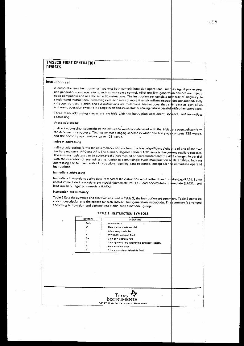
TMS320 FIRST:GENERATION DEVItES
instruction set
A comprehenstve instruction set suppons both numeric-intensive operations, as signal processing. and general-purpose operations. such as high-speed control. All of the fir:st-gene:rati~Jn devices are object-code compatible and use the same 60 tnstructions. The instruction set of single-cycle single-word instructions. permitting execution rates of more than six million second. Only infrequently used branch and I 0 .nstructtons are multicycle. Instructions that as part of an arithmetic operation execute in a single cycle and are useful for scaling data in other operations.
Three main addressing and immediate addressing.
direct addressing
In direct addressing. seven bits of the instruction word concatenated with the 1 -bit the data memory address. This implements a paging scheme in which the first and the second page contains up to 128 words.
indirec~ addressing
Indirect addressing forms the d2:a memory address from the least-significant eight auxiliary registers, ARO and AR1. The Auxiliary Register Pointer (ARP) selects the The auxiliary registers can be au10matically incremented or decremented and the with the execution of any indirect instruction to permit single-cycle manipulation addressing can be used with all instructions requiring data operands, except for instructions.
immediate addressing
Immediate instructions derive data from :Jan of the instruction word rather than useful immediate instructions are multiply immediate (MPYK), load accumulator irrlfn•>rli:•t<• load auxiliary register immediate ilAR!(I.
instruction set summary
Table 21ists the symbols and abbreviations used in Table 3, the instruction set ""'m'""'"' a short description and the opcode for each TMS320 first-generation instruction. accordirig to function and alphabetized within each functional group.
ACC 0 I
K
PA
R
s X
TABLE 2. INSTRUCTION SYMBOLS
Accu:r.ula':or
Data me~ory address field
Ac:oress•ng mode bit
lmf"l"'edia~e operand field
3-btt por. acoress field
l-b1t opera11C: field specifying auxiliary register
4-b,t lef'::-srutt code
3-twl ac=u..,wla~or lett-shift field
TEXAS -l.f} INSTRUMENTS
1 -,· L-:: .... )'-1
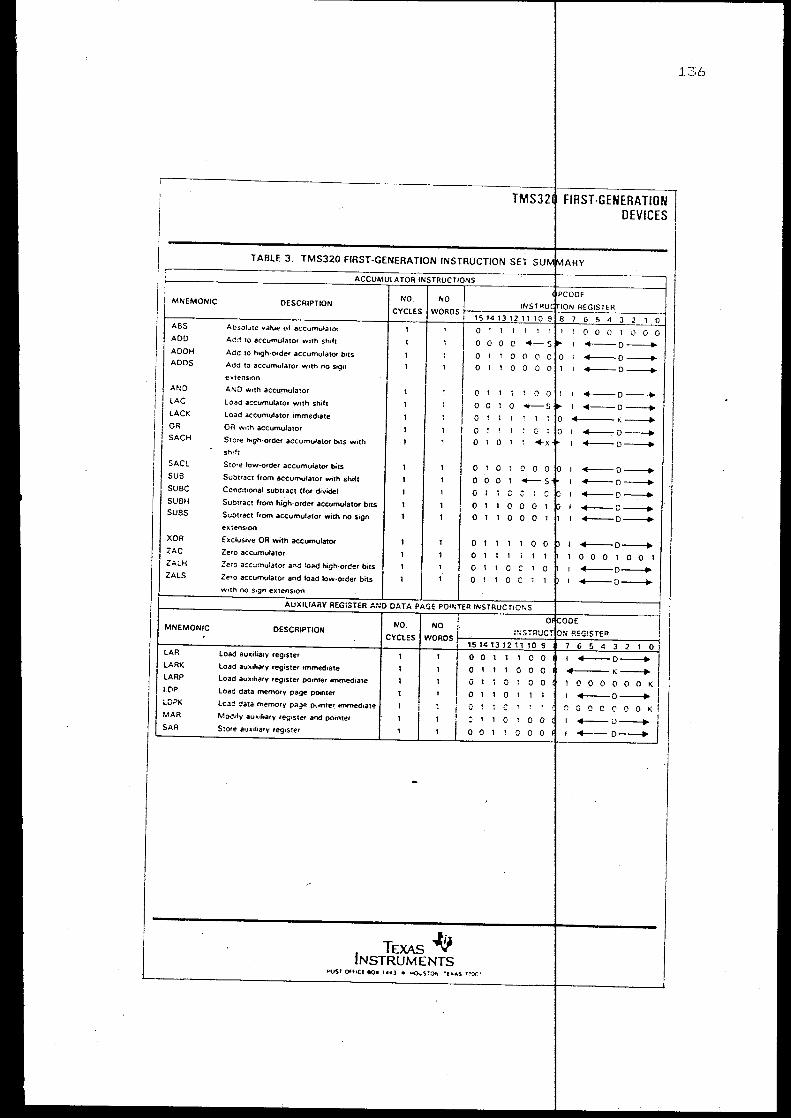
MNEMONIC
ABS
ADO
AOOH
ADOS
AND
LAC
LACK
OR
SACH
SACL
SUB
SUBC
SUBH
suss
XOR
ZAC
ZALH
ZALS
MNEMONIC
LAR
LARK
LARP
1.(\P
t.OPK
MAR
SAR
DESCRIPTION
Absolute volue of accumu~atOf
Add to accumulator w1th stuft
Ada 10 htgh-order accumulator b•ts
Add to accumulator Wtth no stgn
e .. tens•on
AND Wtth accumulator
Load accumulator with shift
Load accumulator immedtate
OR w1th accumulator
Store htgh-order accumulator b•ts w1th
Shift
Store klw-order accumulator bits
Subtract from accumulator with shift
Cond,bonal subtract Uor dtvtdeJ
Subtract from high-order accumulator bits
Sut>tract from accumulator with no sign
eAtension
Exclusive OR with accumulator
Zero accumulator
ze~o a::c~mutator 31'\d !oad high-order bits
Z-ero accumulator and toad Sow-order bits
DESCRIPTION CYClES
load auxthafy register
load auxiliary register tm~1ate
load au••hary reg•ster pornter tmmed•ate
load data ~mory page p~nter
lead data memory pa~ p-;cnrer tmmedaat~
M(hj,fy auxiltary reg•ster and pointer
Store auxrliary reg1ster
TEXAS Jj} INSTRUMENTS
0 1
0 0 0
0 1 1
0 1 1
0 1
0 0
0 1
0 ! !
0 0
0 1 0
0 0 0
0
0 0 1
0
0 1
0
0 0
0
0
0 .·.
' ' 0 0
TMS32 FIRST-GENERATION DEVICES
1 1 1 0 0 0 1 0 0 0 c ._s -0-0 0 0 0 0 1 -0-0 0 0 0 1 I -0-
0 0 -0-0 +--0-K--0-1 +--o-
1 -0--0-v ,. +--o-0 0 0 +--D-----... 0 0 +--o-
0 +--D--+ 1 0 0 0 1 0 0 1
0 c +--o-0 c +--D-
0 0 +--o-0 0 0 K-0 0 0 0 0 0 0 0 0 K
0 1 +--0-
- ~ 0 0 0 0 0 0 K
0 0 0 -l)-! 0 0 0 -4-- 0---+
136
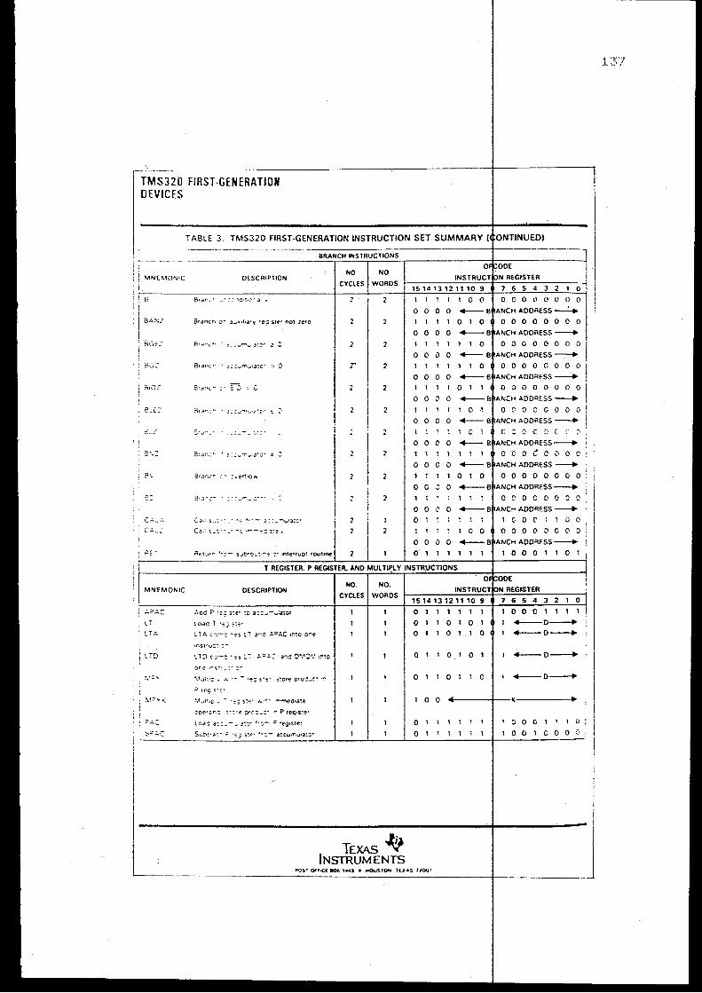
!
TMS320 FIRST-GENERATION DEVICES
TABLE 3. TMS320 FIRST-GENERATION INSTRUCTION SET SUMMARY
MNEMONIC
6
8~:'\:Z
5GE:
6G:
tH02:
E ... ::_
---S'.:
3\
--c..:. --\..- _ ...
~=~
MNEMONIC
s=-:..-.:
DESCRIPTION
Brar'l.-:,.._ ~. ::: _,t:·~ .;:•' i)
Br~H1Cr"'l o- ~--·l·a·, •e9 st~~ not le<O
Sranc .... :::.;mw.a~:-- ~ :l
Branc,.. =::...,m ... :a:c· > 8
6rdn(.."' :.J c
3r ~~n::: ... ? : : ...;"'•· •• ·.:= ~ .::·.
-d"" .. - - --
3:a;::.""' ;::..;"':"'-~a~:·
Branc ... :.ed•c<A
e~J ... :::- . - ·--
(a:: s_:·:_· ···- ::: :_-"" .... i3!-:•
(ail ~-=.- . - ~:~ ...
DESCRIPTION
.:..oc P ~~;: s:~· -:c a:c--:..,:a:or
Loao T -~: s:er
•nstruc-:-
NO NO
CYClES
r
2
2
2
2
1
2
CYClES
LTO c:-: -es :._"':'" .:.~:.: 3!':.~ !)~.4 QV :!"'!~0
? reg·s:~·
TEXAS~ INSTRUMENTS
0 1
0
1
0
0
0
1
0
1
0
1
0
1
0
0
0
1
0
0
0
0 1
0
0
0
0
0
0
0
1
0
0
0
0 0
1
0 0
u 0
0 0
,. 0
c 0
0 0
c 0
;; 0
0 0
0
0 0
0 t 0 t 0
0 0
0 0
0 1
0 1 ,
0
1. :~;7
.__0_
.__0_
, 0 0 0 1 , 0
0 0 0 0 0 0
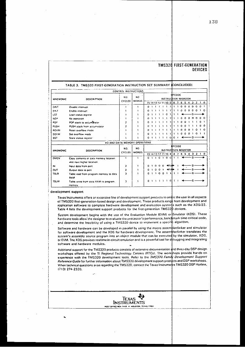
MNEMONIC DESCRIPTION
OtNT O•sable .nteuupt
E!NT Enable tnterrupt
LST Loa:1 ~tatus reg•s:er
NOP No operatton
PO? POP stack to accum\!ator
PUSH PUSH stack from accumulator
ROVM Reset overflow node
SOVM Set overflow mode
SST Store status reg•ster
MNEMONIC DESCRIPTION
DMOV
IN
OUT
TBLR
Copy contents of data memory tocation
&r:to neKt h•gher locat•on
Input data from port
Output data to port
Table read hom program memory to dala
RAM
NO NO
CYCLES WORDS
2
CYCLES
2
3
0 1 1 1 I
0 1 1 1 1
0 1 1 1 1
0 1 1 1 1
0 1 1 1 1
0 I 1 1 I
0 1 1 I 1
0 1 1 1 1
0 1 1 1 1
0 1 0 0 0
0 1 0 0 1
1
1
0
1
1
1
1
1
0 1 {) 0 1
1
1
1
1
1
1
1
I
0
FIRST-GENERATION DEVICES
1 1
1 1
1 I
1 1
1 1
1
1 1
1 1
0 I
0 0 0 0 0 0 1
0 0 0 0 0 1 0
-D--+
0 0 0 0 0 0 0
0 0 I 1 0 1
0 0 1 1 1 0 0
0 0 0 0 0
0 0 0 1 0 1 1 -D-.__D_ .__0_ -0--+
TSLW Table write from cat a RAM to program
memorv
3 0 1 i 1 1 C 1 I -0--+
development support
Texas Instruments oHe:s an extensive line of development support products to of TMS320 first-generation-based design and development. These products application software to complete hardware development and evaluation Table 4 lists the development support products for the first-generation TMS3
System development begins with the use of the Evaluation Module (EVMl or
the user in all aspects from development and such as the XDS/22.
{XDSl. These
hardware tools allow· the designer to evaluate the processor's performance. hpnr·lllrn,.rk
and determine the feasibility of using a TM$320 device to impiernent a
Software and hardware can be developed in parallel by using the macro ""'"'"'m~''"'·/lu-.k., for software development and the XDS for hardware development. The '""~"rnllliPrllrr>kf!f system's ass.embly source program into an object module that can be or EVM. The XDS provides realtime in-circuit emulation and is a powerful tool for software and hardware modules.
and simulator
Additional support for the TMS320 products consists of extensive documentation thre~-day DSP design workshops offered by the Tl Regional Technology Centers (RTCsl. The uur""·lh,mc provide· hands-on experience with the TMS320 development tools. Refer to the TMS320 Support Reference Guide for further information about TMS320 development support and DSP workshops. When technical questions arise regarding the TMS320. contact the Texas rn~mrm<>n TMS320 DSP Hotline.
1713) 274·2320.
TEXAS -lj} INSTRUMENTS
f"OSf ()HIC( iM).I( 1443 e HOuStON. t(XAS 77001
138
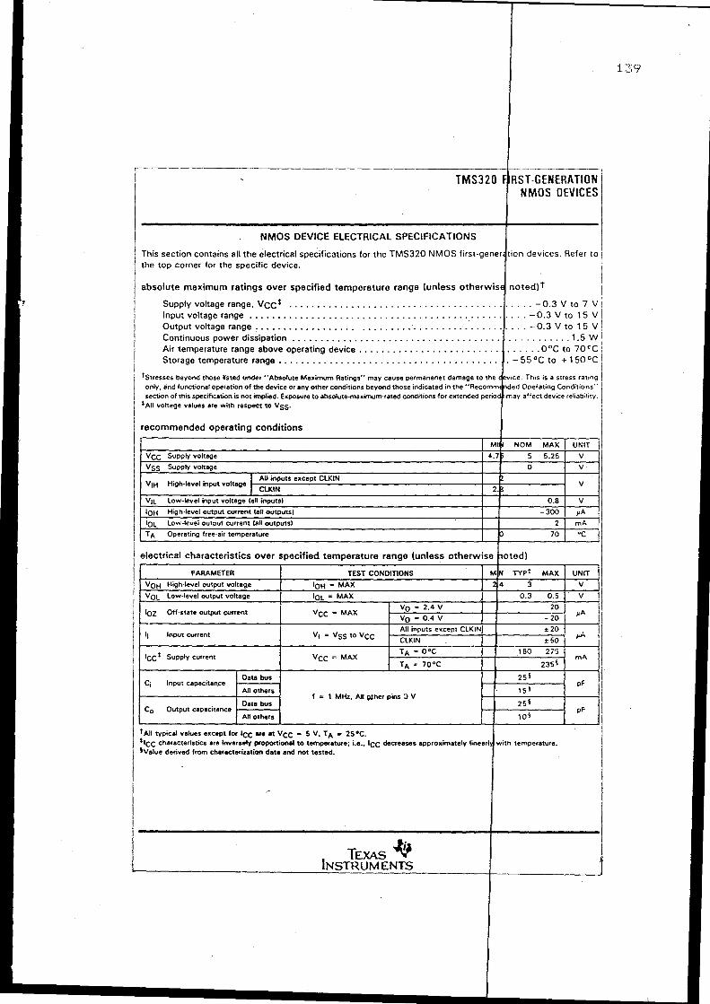
TMS320
NMOS DEVICE ELECTRICAL SPECIFICATIONS
This section contains all the electrical specifications for the TMS320 NMOS the top corner for the specific device.
absolute maximum ratings over specified temperature range (unless otherwis
Supply voltage range, Vcct ..................................... . Input voltage range ............................................. . Output voltage range , .......................................... . Continuous power dissipation .................................... . Air temperature range above operating device ........................ . Storage temperature range ...................................... .
1stresses beyond those listed under uAbsolute Maximum Ratings .. may cause permananet damage to the
-GENERATION II'
NMOS DEVICES
. .. -0.3 V to 7 V
. . -0.3 V to 15 V . .. -0.3 V to 15 V
. . . - ..... - .1.5 w . . . . . . 0°C to 70"C . --55°Cto +150°C
. This is a stress rating only, 8nd functional operation of the device or any other conditions beyond those indicated in the '"Rec<lml-n<jnd<•d section of this specification is not implted. Exposure to absolute-maximum-rated conditions for extended
tAll voltage values are with respect to Vss-
recommended operating conditions
electrical characteristics over specified temperature range (unless otherwise
II Input current v1 = Vss to Vee
'cct Supply current Vee~ MAX
Ci Input capacitance
f = 1 MHz. All I)Zher pins :> V Co Output capacitance
'An typical values except for tee ere et Vee • 5 V. TA • 25"C. *tee characteristics are inversely proportional to temperature: i.e ... tee decreases approximately tvalue derived from characterization data end not tested.
TEXAS -I!} INSTRUMENTS
pF
pF
with temperature.
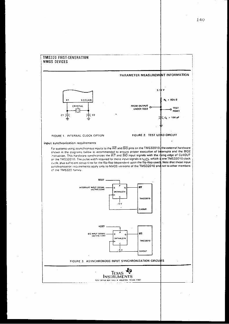
t TMS320 FIRST-GENERATION NMOS DEVICES
XI X2/ClKIN
2. v
RL = 825 ll
FROM OUTPUT o---· UNDER TEST .. --.0 TEST
POINT
Cl~ ~C2
FIGURE 1. INTERNAL CLOCK OPTION FIGURE 2. TEST
input synchronization requirements
For systems using asynchronous inputs to the INT and 810 pins on the TM$3201 external hardware shown in the diagrams below is recommended to ensure proper execution of ,,.,.,.rrumr~ and the BIOZ :nstruction. This hardware synchronizes the !NT and 810 input signals with the edge of CLKOUT or. the TMS320i 0. The pulse width required for these input signals is tc(C). which one TMS32010 clock C> cle, plus suffocient setup time for the flip-flop {dependent upon the flip-flop S>nchronization re::Juirements apply only to NMOS versions of the TM$32010 o~ :he TMS320 family.
INTERRUPT tNPUT SIGNAl 1ACTIVE lOWl
810 INPUT SIGNAl !ACTIVE lOWJ
I p
ol----o Slf7 .. AlS7 ..
r-~ c
I ·S v
iNf
TMS32010
ClKOUT
TMS32010
FIGURE 3. ASYNCHRONOUS INPUT SYNCHRONIZATION
TEXAS -l.jJ INSTRUMENTS
140
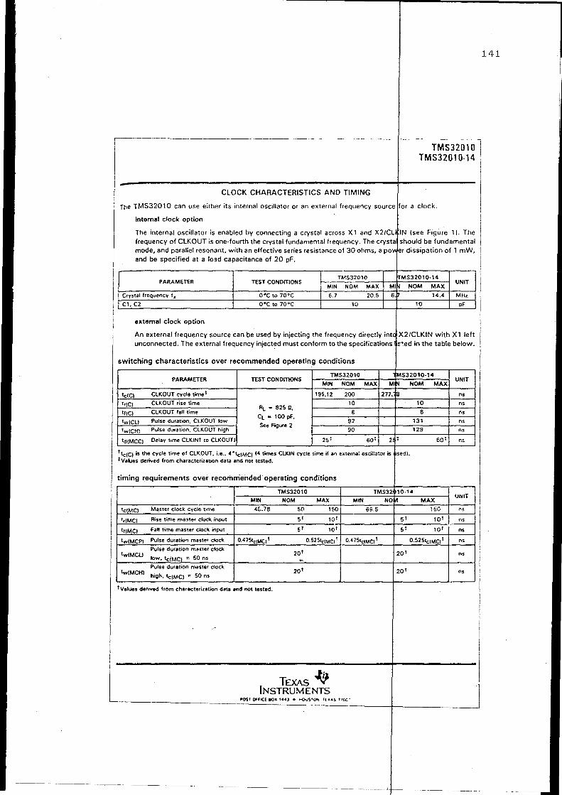
1.41.
i
I .--~
TMS32010 i TMS32010-14 I
CLOCK CHARACTERISTICS AND TIMING
The TMS320 10 can use either its internal oscillator or an external frequency source ~or a clock.
internal clock option
The internal oscillator is enabled by connecting a crystal across X 1 and X2/CL IN (see Figure 1). The frequency of CLKOUT is one-fourth the crystal fundamental frequency. The crysta should be fundamental mode, and parallel resonant, with an effective series resistance of 30 ohms, a poVI er dissipation of 1 mW, and be specified at a lo3d capacitance of 20 pF.
TMS32010 TMS32010·14 PARAMETER TEST CONDITIONS
Ml~ UNIT
MIN NOM MAX NOM MAX
Crystal frequency f x o•c to 1o•c 6.7 20.5 6. 14.4 Mflz
C1.C2 o•c to 1o•c 10 10 pF
external clock option
An external frequency source can be used by injecting the frequency directly intc , X2/CLKIN with X 1 left unconnected. The external frequency injected must conform to the specifications !:'•ed in the table below.
switching characteristics over recommended operating conditions
TMS32010 MS32010-14 PARAMETER TEST CONDITIONS
Mr. UNIT
MIN NOM MAX NOM MAX
lciCI CLKOUT cycle timet 195.12 200 277. :8 ns
'riC! CLKOUT rise time 10 10 ns
tfiCI CLKOUT fall time RL : 825 ll,
8 8 ns
twiCLI Pulse duration. CLKOUT low CL = 100 pF.
92 131 ns
Pulse duration. CLKOUT high See Figure 2
90 129 twtCHl ns
ld!MCCI Delay time CLKINI to CLKOUTI 25: 60: 2 ,f 60 1 r.s
1tc(CI is the eycle Time of CLKOUT. i.e .• 4•tc(MCI 14times CLKIN cycle time if an external oscillator is 1Values derived from characterization data and not tested.
sed).
timing requirements over recomni~ehded operating conditions
TMS32010 TMS32 10-14 : UNIT 1 I MIN NOM MAX MIN NO_. MAX
tciMCI Ma;ster clock cycle time 4£..78 50 150 I 69.5 150 I ns
1riMCI Rise time master clock input sl 10' s' ~~ tf!MCI Fall time master clock input s' 101 st 101 ns
lw(MCPI Pulse duration master clock 0.47StciMCII 0.5251cfMCI I 0.475tc!MC! I 0.52StciMCI 1 ns
Pulse duration master clock 201 20' lw(MCLI ns
low. '<:!MCI = 50 ns -Pufse duration master clock 20 1 20' tw(MCHI ns
high. '<:IMCI = 50 ns
tvatues derived from characterization data and not tested.
'
I
l TEXAS lj} ·1 INSTRUMENTS _j f»()St ()Ut(( BOX t6•J e ..cAIS"at. f(AAS 11(1("
---- ~ ~ --- ~-- - ---- ---~ ----~-- -~ -~-- --- --~- ----- -~ . ~ -- - ------ ~- ~-- -----
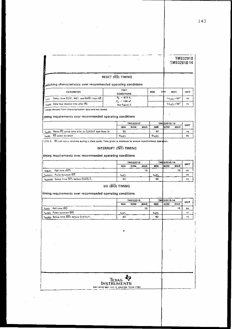
RESET (RSI TIMING
·\'aloes derivej from characterization data and not tested.
TEST CONDITIONS
RL = 625 0.
CL = 100 pF.
See Figure 2
timing requirements over recommended operating conditions
TEXAS~ INSTRUMENTS
MIN
TMS32010 TMS32010-14
1.4::;
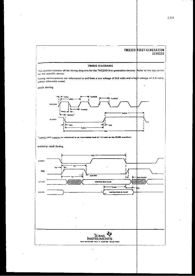
TMS320
TIMING DIAGRAMS
-GENERATION DEVICES
This section contains art the timing diagrams for the TMS320 first-generation devices. to the top corner tor the specific device.
Timing measurements are referenced to and from a low voltage of 0.8 volts and a voltage of 2.0 volts, unless otherwise noted.
clock timing
-+t ,.. 'nMCI ...----ef" lwiMCHI
tr-'ciMCI~ I
X21ClKtN . . . : I J.----.1- lw(MQ.f
··~r.oa...J ..... L.-.,- .... MCCI r
,.... _____ '-<Ott ---1--
CLKOUT
~~-------------------', -.l 1.- 'ffCI -.l ~ "<a
: ...._ ____ '.olCI.•------tol 14------------tclCI--------------11---+1
''dtMCCI •nd !w(MCPI ••e referenced to an intermediate level of 1.5 volts on the CUCIN w..,eform.
memory read timing
ClKOUT
A11-AO
01$ DO
TEXAS -lj} INSTRUMENTS
144
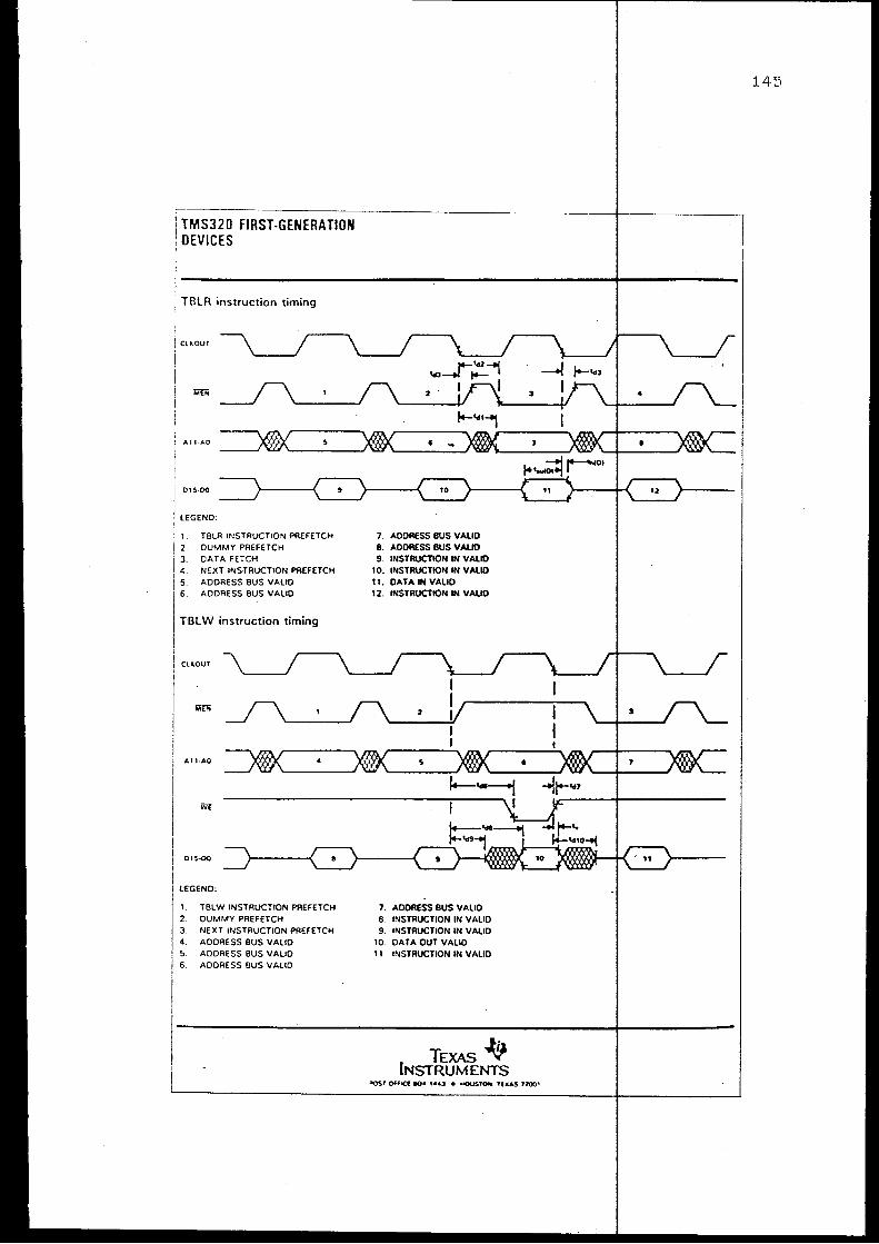
TMS320 FIRST-GENERATION DEVICES
TBLR instruction timing
ClKOUl
A11-A0
LEGEND:
1 TBLR INSTRUCTION PREFHCH 2. DUMMY PREFETCH 3. DATA FETCH 4. NEXT INSTRUCTION PREFETCH 5. ADDRESS BUS VALID 6. ADDRESS BUS VALID
TBLW instruction timing
CUC.OVT
A11·A0
015-00
LEGEND:
1. TBl W INSTRUCTION PRE FETCH 2. DUMMY PREFETCH 3. NEXT INSTRUCTION PREFETCH 4. ADDRESS BUS VALID 5. ADDRESS BUS VALID 6. ADDRESS BUS VAliD
7. ADDfiESS BUS VALID 8. ADDRESS BUS VALlO 9. INSTRUCTION IN VALlO
10. INSTRUCTION IN VAllO 11. DATA IN VALID 12. INSTRUCTION IN VAllO
7. ADDRESS BUS VAllO 8. INSTRUCTION IN VAllO 9. INSTRUCTION IN VALID
10. DATA OUT VAliD 11 INSTRUCTION IN VALID
TEXAS JjJ INSTRUMENTS
14!'..1
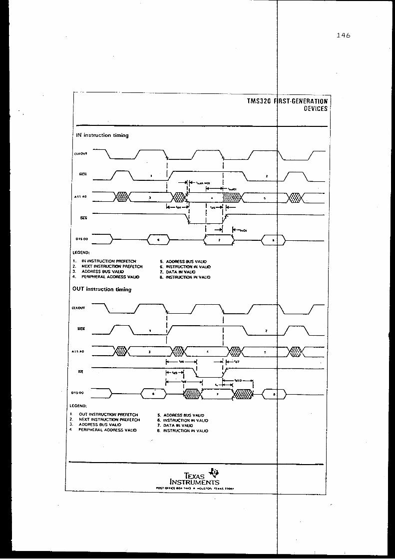
IN instruction timing
CLKOUl
A11-A0
015·00
LEGEND:
1. IN INSTRUCTION PREFETCH 2. NEXT INSTRUCTION PREFETCH 3. AOORESS BUS VAllO 4. PERIPHERAL ADDRESS VAllO
OUT instruction timing
ClKOUT
A11-AO
015-00
LEGEND:
1. OUT INSTRUCTION PREFETCH 2. NEXT INSTRUCTION PREFETCH 3. ADDRESS BUS VAllO 4 PERIPHERAL ADDRESS VAllO
5. AOORESS BUS VAllO 6. INSTRUCTION IN VALlO 7. DATA IN VAllO 8. INSTRIJCTIOH IN V AliO
5. ADDRESS BUS VAllO 6. INSTRUCTION IN VALID 7. DATA IN VAllO 8. INSTRUCTION IN VALID
TEXAS 'l!J INSTRUMENTS
TMS320 -GENERATION DEVICES
1.46
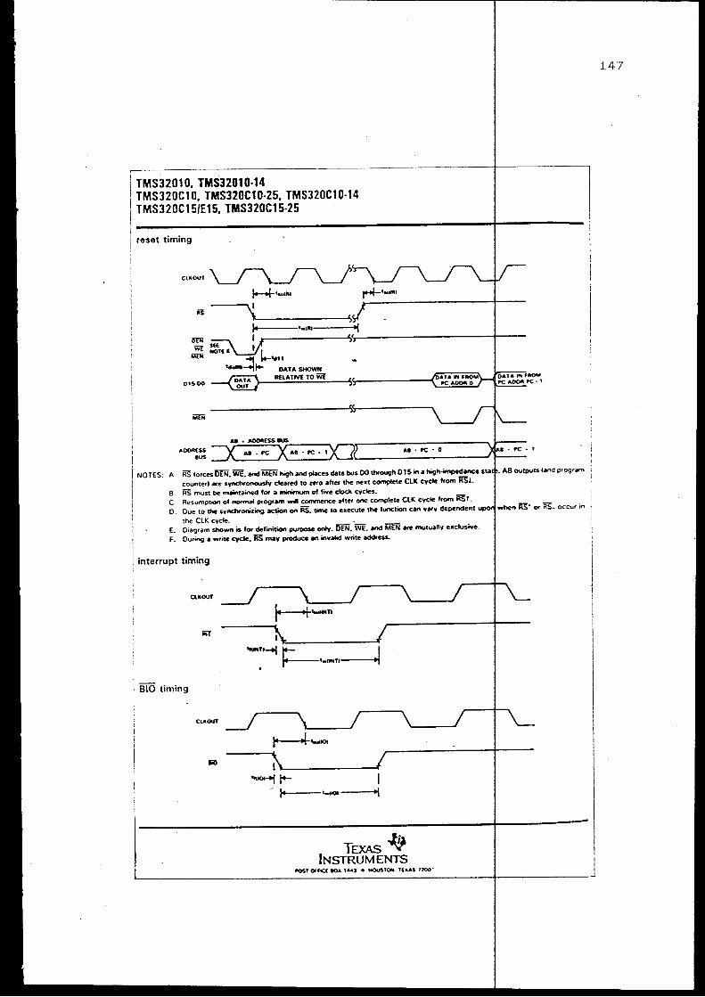
TMS32010, TMS32010-14 TMS320C10, TMS320C10-25, TMS320C10-t4 TMS320C 15/£15, TMS320C15-25
reset timing
Ct«.Ol11
K ....... , ---.....
01S-DO
AOORESS eus
OATASHOWN RElATIVE TOW[
NOTES: A RS torces DEN. WE. and MEN t.;gh and places data bus 00 thtougl\ 015 in a high·impedance counterl are sync:t..onously cleated to zero after the next complete CLK cycle from RS1.
B. RS must be n>Mtained f01 a rNnimum of five clock cycles. C. Resumption of nonnal program will commence after one complete CLK cycle from RS!. 0. Due to the svnclvonizin9 action on RS. lime to execute the function can vatv dependent
:he CLK cvcle. • E. Diagram shOwn is fOI definition purpose only. om. WE. and MEN Me mutually e•clusive. F. During a wr;ce cycle. RS may produce an invalid write address.
interrupt timing
ClKOUT
BIO timing
ClKOUT
I "-------~ ... ~ t+- I
- Hl4>----•-oeot---_.,"i
TEXAS Jj} INSTRUMENlS
147
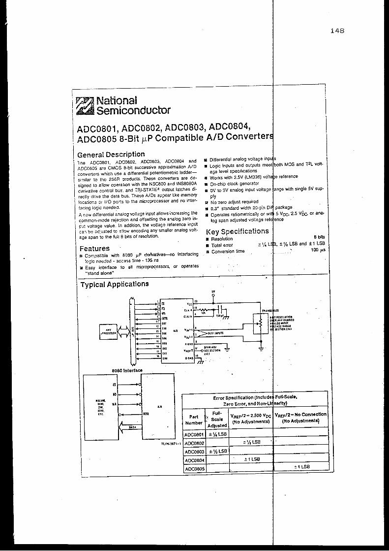
wNational Semiconductor
ADC0801, ADC0802, ADC0803, ADC0804, ADC0805 8-Bit J.LP Compatible A/D Converte
General Description The ADC0801, ADC0802, ADC0803, ADC0804 and ADC0805 are CMOS 6-bit successive approximation AID converters which use a differential potentiometric laddersimilar to the 256R products. These converters are de· signed to allow operation with the NSCSOO and INSSOSOA derivative control bus. and Tf'!I-STATE~ output latches di· rectly drive the data bus. These AIDs appear like memory locations or i/0 pc:-~ to the micro.processor and no intere
facing logic needed. A new differential analog voltage input allows increasing the common-mode reieC"Jon and offserJng the analog zero input voltage value. ln addition, the voltage reference input can be adjusted to a:low encoding any smaller analog volt· age span to the full 6 b.'ts of resolution.
Features t1 Cor.1patible with 8030 1-1? denvat'ves-oo interlacing
log!c needed. ac:-ass tjme- 135 ns u Easy interlace to all microprocessors. or operates
"stand alone"
Typical Applications
II .. ,c
" CLJ. A
tLJ:I"'
.... v1,.t•l
v111 1-l ' I
8080 Interface
C1
~
JCSCIIG. l<liO, Wl ,ltl. .. .. &041, ETC. ~
Part A .... '{
~
11 Differential analog voltage a Logic inputs and outputs m~·ntlhr>·th MOS and T2L volt-
age level specifications II Works with 2.5V (LM336) • On-chip clock generator a OV to SV analog input voltage
ply 1o1 No zero adjust required 11 0.3' standard width 20-pin 11 Operates ratiometrica:ty or
'"'
log span adjusted voliage
Key Specifications a Resolution 11 Total error Ill Conversion time
••
Olff lkt\ITS
Zero Error,
-:
with single SV sup-
8bi1s ±% LSB and ±1LSB
100 p.S
Full- VREF/2= 2.500 Vee VREF/2=No Conneetlon (t{o Adjustments) (No Adjustments}
148
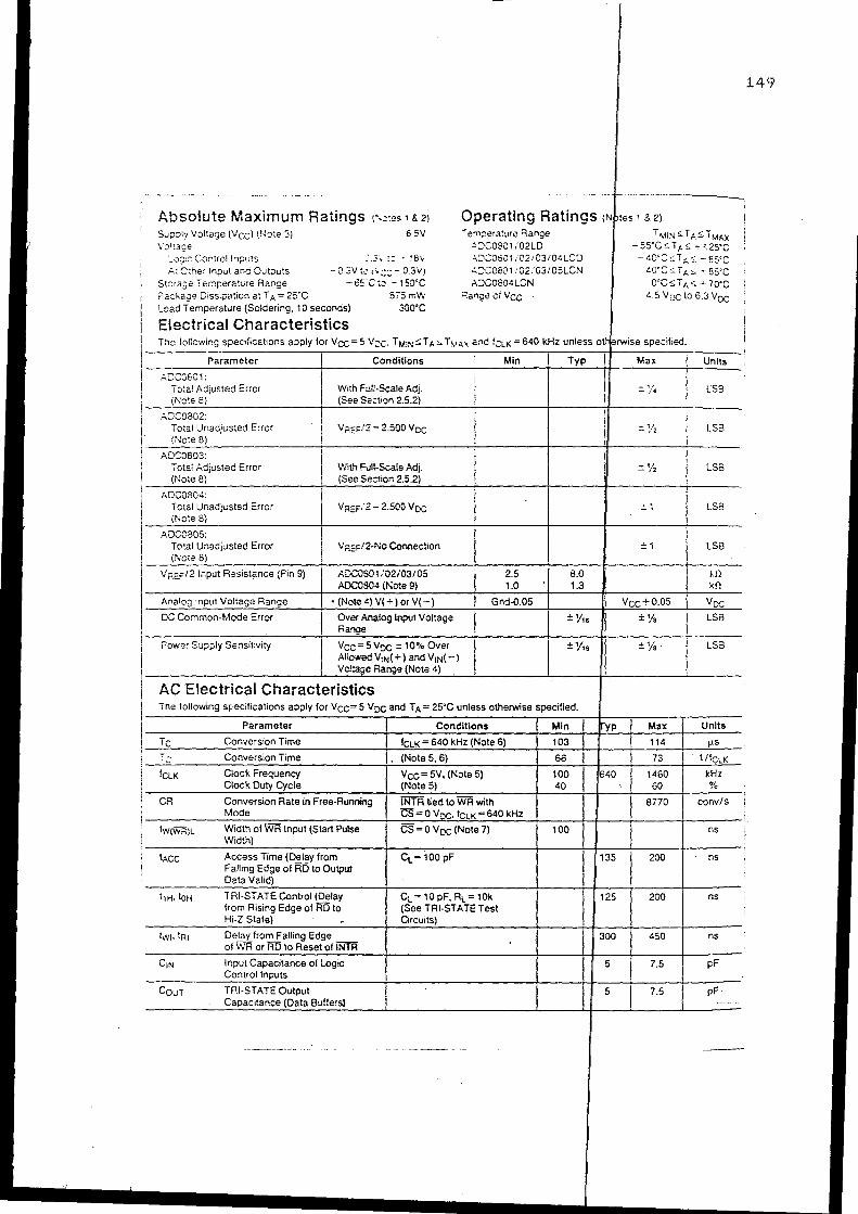
Absolute Maximum Ratings t•,::es 1 & 21
Sup:;ly Voltage (Vee) {NQte 3~ € SV
Operating Ratings <
:...o:;:: Controlt~puts A: Cther Input and Outputs
Stora~e Ter.1perature Range ?acka::;e 01ssipation at T A= 25'C
·· 0 .3V 10 i ·• :;:; - G.3V} -c::·c:.J -1socc
575mW Lead Temperature (Soldering, 10 seconds) 300'C
Electrical Characteristics
AOC0801: To:a! Adjusted Error
8)
ASC0802: Total Unadiusted Error (Ncte
ADC0803: Total Adiusted Error (Note 8)
ADC0804: Total Unadjusted Error
ADC0805: Total Unadjusted Error (NoteS)
VREF/2 Input Resistance (Pin 9)
Power Supply Sensitivity
With F:.>I!-Scale Adj. (See Sectior, 2.5.2)
With Full-Scale Adj. (See Section 2.5.2)
V?.EF· 2= 2.500 Yoe
Y;:;E"/2-No Connection
AIX-"0501 /02/03/05 ADCOSO-' (Note 9)
Vee= 5 Yoc = 10% Over Allowed YtN( +)and Y:N(-)
AC Electrical Characteristics
""em='erature 8ange .;:)C0801 /02LD .;:)C:C'S01 i02103i0~LCD . .;::;C0801 /02:'03/0SLCN A:JCC604LCN
;:::ange of Vee
2.5 8.0 1.0 1.3
:::y,6
±y,.
The following SJ:.·ecifications apply for Yec=S Voc and TA = 25'C unless otherwise specified.
CR Conversion Rate in Free-Rur.ning Mode
tw(WR}l Width of· Input (Start Pulse CS=OYoc(Note7) 100 Wid:h)
tAee Access Time (Delay from CL =iOOpF Falling Edge of RD to Output Data
l1H. toH TRI-STATE Control (Delay CL =10pF, RL =10k from Rising Edge of RD to (See TRI-STATE Test Hi-Z State)
tw1.tR1 Delay from Falling Edge __ of WR or RO to Reset of INTA
CtN Input Capacitance of Logic Control Inputs
Cour TRI-STATE Output Capac1tance (Data Buffers}
-----~---- ··- -------
135
125
300
5
5
, &2)
T MiNS:T .t.:STMAX -ss·co::T;.$ +'12S'C ~t.o~c::TA.o:~ -sscc -.!O'C$TA,;, -85'C
O'CS:TA 0:: + 70'C t:.5 Yoc to 6.3 Voc
= ~~ LSB
:: :;2 LS3
::':'/, LSB
:=1 LSB
±1 LSB
U)
kf!
±'is LSB
:':'/s LSB
~{.
8770 conv/s
ns
200 ns
200 ns
450 ns
7.5 pF
7.5 pF·
149
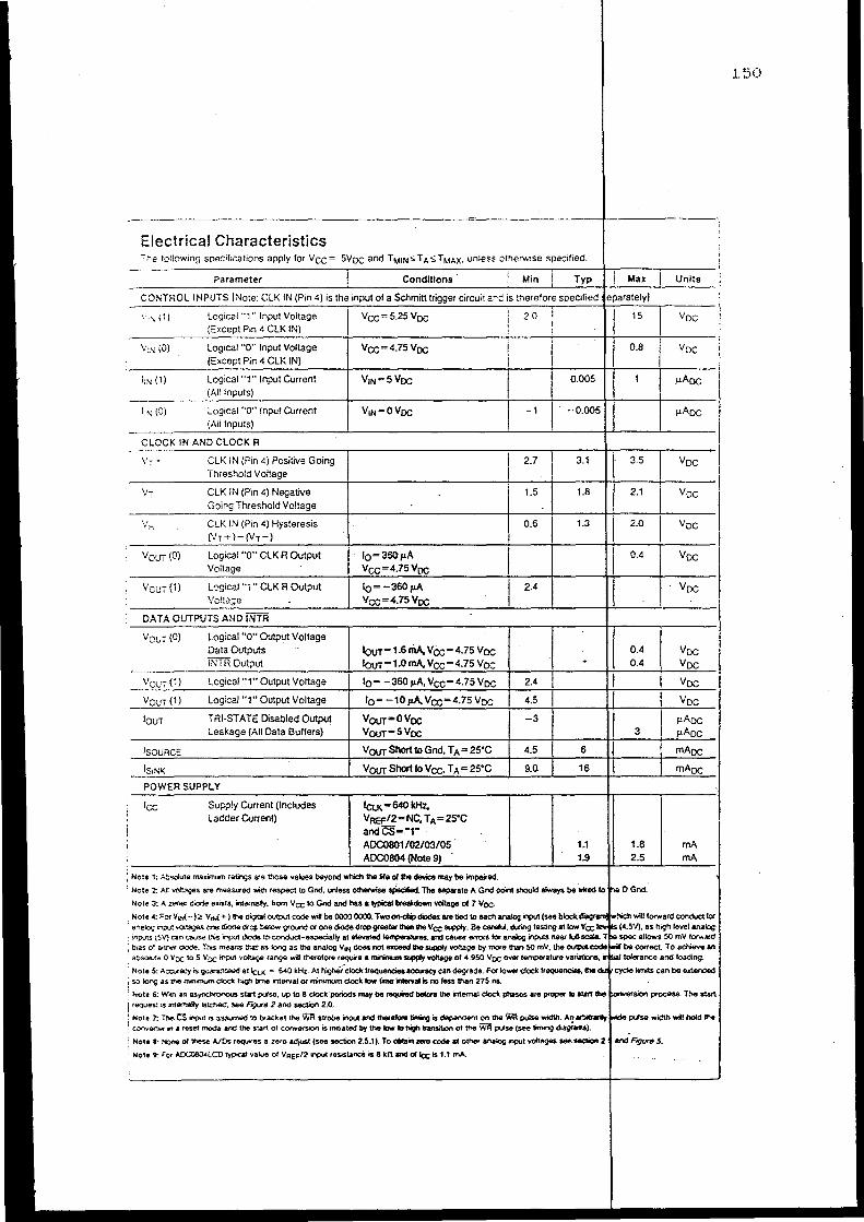
Electrical Characteristics I he following specifications apply for Vee= SVoc and TMIN,;TA,;TMAX· unless otnerv.·1se specified.
'.',, (1)
V:.N(O)
llN(1)
I.N (0)
v,-
Vr-
v,.,
VoUT (0)
Veur(1)
Voui (O)
Icc
Logical''1''1nput Voitage (Except Pin 4 CLK IN)
Logical "0" Input Voltage [Except Pin 4 CLK IN)
Logical"1" Input Current (AIIInpu1s)
Logical "0" Input Current (All Inputs)
CLK IN (Pin 4j Positive Going Threshold Voltage
Going
CLK IN (Pin 4) Hysteresis (Vr+)-(Vr)
Logical "0" CLK R Output Voltage
Logical"1" CLK R Output
logical "0" Oulpu1 Voltage Data Outpu1s iNTROutpu1
Supp!y Current (Includes Ladder Current)
Vcc=5.25Voc
Vcc=4.75 Voc
V1N=5 Voc
V1N=OVoc
fCLK = 640 kHz, VReF/2=NC, TA=25'C andCS="1" ADC0801/02/03/05 .
ADC0804
Note 1: Absolute maJcimum ratings are those values beyond which the life ol the cte.ice may be impaired
2.0
-1
2.7
1.5
0.6
2.4
0.005
-0.005
3.1
1.8
1.3
1.1 1.9
Note 2: All vol'.a;;es are rMasu-ed wilh respect 10 Gnd, unless othetwise Sjiecified. The saparate A Gnd point should always be Wed
Note 3: A zeMt dio<j;o erists, in!Otna,ly, from Vee to Gnd and has a typical II<-voltage ol7 Voc
15
0.8
3.5
2.1
2.0
0.4
0.4 0.4
1.8 2.5
Note~: Fe< V.,..{-);, V,..(+) tt.e d9'<aloutp1.1 code will be 0000 0000. Twoon-cl>pdiodes are lied 10 each analoqinou1 {!;eeblockc!ac"""o!lwhic!l a oak>\; "'pol "ll= C<'e dK>de dr~ below ground or one diode drop greala' a- lll8 Vee supply. Be ea<elul, d«ing testing at inputs t5V} can r_~ !:\'S irput dtode. W condvct-especia.lfy at elevated tempera.es. and cause emxs 1« anaklg inputs near
bias o! "'"""diode. This ~ns ,..., as long as lhe analog v.., does not eu:aedllle supply IIOI!ag<~ by more INn SO mV, the a~soMe 0 Voc tQ 5 ~·oc in;><rt vo~>age ra"9" will th<KefO<e require a rnft1imum supply voltage of 4.950 Voc ovet temperature
Note 5: ACOAacy ;,; ~"eed at fct.k - 540 kHz. At h~ clock frequencies acancy can degrade. Fe< low« clock lrequenc;.s. so long as lt.e min""""' clock toq. ..,., nte<Val or minimum clock tow lime inlonlal is no less ltlan 275 ns.
. Note 6: W-"' •" esyoct><O<'OUS start pUSO, up to 8 clock periods may be roquHclbolore the internal clock phases are proper II> SUit 1lle
i '"'l'""" <S .mernalty laW'.ed. se.~ F'flJTB 2 and S<ldion 2.0.
Voe
V:x
J-LAoc
J-LAoc
Voc
Voe
Voe
Voe
Voc
mA mA
process. The SWt.
: Note 7: '""' CS "'''Uf <S assume<! !o b<acket the WI\ strobe input and !hot- fim;ng is depeOOent on lhe W!i pulse width. Af! .v..i-ilv~.;de pulse width will hold the ·~ cOrtverter _, a reset rnoct.e and the start ol cOt'IWWsion ts initiated by the low D high tRln:sibon of tne WR puts& (see timing d1agqm.5).
:Note 1: None ott"""' "-'Ds requo-es a ze<o acfJUSt (see section 2.5.1). To olllainzerocode at otner anologonput voltages set<HCticn
Note 9: Fer AOC060-<LCD typical value of VRer/2 onput resistance is 8 kfi and of lex: is 1.1 mA.
150
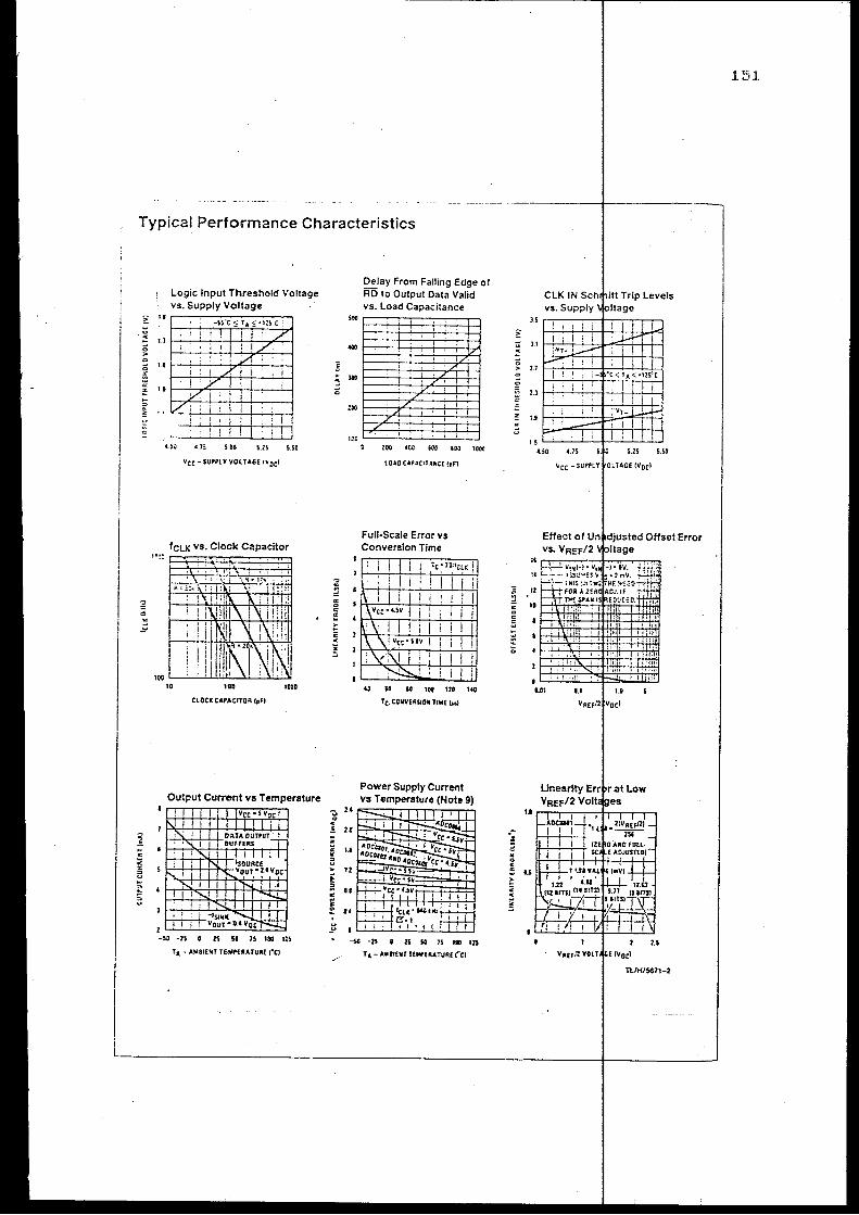
Typical_ Performance Characteristics
~
·~ > 0
0 %
" %
" L
"" ~
"' .s ... " " " " u ... " " 0
11
1.1
1.6
I.S
Logic Input Threshold Voltage vs. Supply Voltage
-ss··csrA-::;•12S c:
'! !j_ ! L : IY·
! ! /1 I . I ' I i y,, \ I _l .VI I I l I
v i I I l I '_l__l \ ! ! ! I !J
'" 500 5.25 sso
Vee-SUPPLY VOt TAGE f't'oct
10 181) 10DO
CLOCK CAPAtiTDR CpF)
~~~~~~--~~~ -so -2s a zs .sa 7S tao us
T.1.- A,_.II£HT THIP£AATUII( 1°()
] > ~ c
" "' 0
~ > ... ;;
~
soo
'"' 300
zoo
1~:
Delay From Falling Edge of RD to Output Data Valid vs. Load Capacitance
' I
' I
' !
I '
zoo '"" ~ 100 1000
lOAD CA'.tCIT A"-C£ fpFJ
Full-Scale Error vs Conversion Time
:I' I I .'c ~ ,~,;;~..: ! J
i ! I I ! il I
I ' ' "' 58 10 100 121 1<0
Tc.CONVERSIO. TIME 1141
Power Supply Current vs Temperature (Note 9)
-54 -:s • n ~ 1s 110 us T A - AM ltt.r JEW! RATURl fCJ
151.
" " c
" ::; ... 0
1.1
.-. " " " " u >-;; .. !
TVH/5671-2
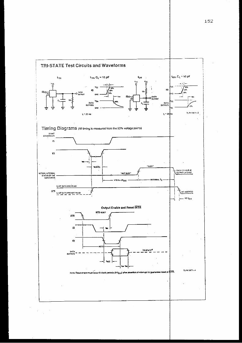
TRI-STATE Test Circuits and Waveforms
_::::H-Vee~~-.9,.._
1!1! SOl\
GNO ~1 0% DATA VoN --='--litH
OUTPUTS ~ CND ------------~
Timing Diagrams (All timing is measured from the 50% vol!aga poi..,:s)
START
tONVERS:ON ----------""'-
Output Enable and Reset UiTR
im\ iiiTJ!AESU ~
jJ B \ I I
Jr.!
Vee
OATA OUTPUT
TRI-STAT£'0
Note: Read Sl700f< must occur 8 clod< p9riods (S/fcu<laHer UMI1ion o< inlemlplto guarantee resel
toH. CL = 10 pf
DATA 'S\'·:~:t.!D"' OUT!'UllJ,'tti'I.E.S
lc:.,.., '\JL
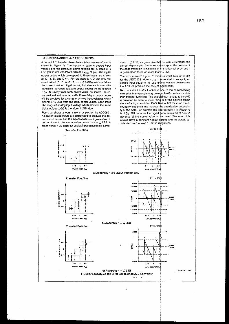
1.0 UNDERSTANDING A/D ERROR SPECS
A perfect A 10 transfer characteristic (staircase waveform) is shown in Figure 1a. The horizontal scale is analog input voltage and the particular points labeled are in steps of 1 LSB (19.53 mV with 2.5V tied to the VREF/2 pin). The digital output codes which correspond to these inpllls are shown as 0-1, 0, and 0+1. For the perfect AID, not only will center-value {A -1, A, A+ 1, .... ) analog inputs produce the correct output ditigal codes, but also each riser (the transitions between adjacent output codes) will be located ±% LSB away from each center-value. As shown, the risers are ideal and have no width. Correct digital output codes will be provided for a range of analog input voltages which extend ± % LSB from the ideal center-values. Each tread (the range·of analog input voltage which provides the same digital outplll code) is therefore 1 LSB wide.
Figure 1b shows a worst case error plot for the ADCOS01. All center-valued inputs are guaranteed to produce the correct output codes and the adjacent risers are guaranteed to be no closer to the· center-value points than ± 't< LSB. In other words, if we apply an analog input equal to the center-
" " ~ 0•1
;! ;; a o-t
Transfer Function
·-·
5Ti I I I I I I I
' I I .. ,
value ~ '/• LSB, we guarantee correct digital code. T11a the code transition is is guaranteed to be no more
The error curve of Figure 1 c for the ADCOB02. Here we g analog input equal to the LSS the AID will produce the correct
Next to each transfer function is error plot. Many people may be than transfer functions. The is provided by either a linear steps of a high resolution tinuously displayed and · ty of the A/D. For example the is + % LSB because the digital advance of the center-value of
"' 0 c
"'
-1/ZLSI
·-· a) Accuracy= ± o LSB A Perfect AID
Transfer Function
the AID will produce the range of the po~itoon of
horizontal arrow and it LSB.
Cef!ter-value
the corresponding familiar with error plots
input voltage to the AID by the discrete output
that the error is conquantiz<ltic>n uncertain-·
point 1 of Figure 1a appeared % LSB in
The error plots the abrupt up-
+I LSI 1----'----lf-
" 0
~ 0•1
E ... ;; Ci D-t
A-1 A.•1
NI.UIG tW\IT (Y,.J
Transfer Function
·-· •••
•liCLSI
"' 0
"' "' -tn LSI
-liCLSI
b) Accuracy= ±%LSB
c) Accuracy= = Y. LSB
--t .. u
~---~~--;<--J~-1- --- r·___ ,
FIGURE 1. Clarifying the Error Specs ot an AID Converter
Tl/HIS61T-12
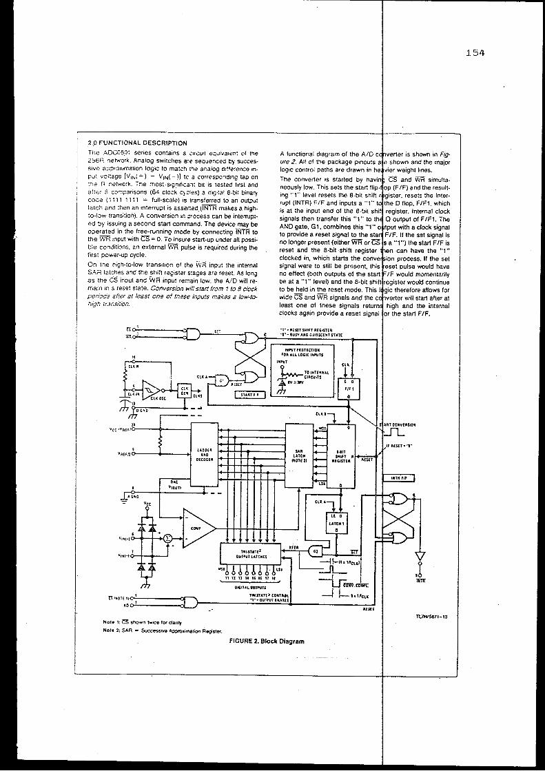
2 .. 0 FUNCTIONAL DESCRIPTION
The ADC08.0, senes contains a c1rcwt equivalent of the 256R net.o.·ork. Analog switches ace sequenced by successive appr:Jx.mation logic to match tr>e analog diffe,ence tnput voltage [V,N( .._) - VIN( -l] tc a correspondtng tap on tr)e R network. The most-sig~·uf1cani b1t IS tested ftrst ana af:E•' 8 comparisons (64 clo.::k c1 cles) a dtgttai 8-bit binary code ( 1111 11 < 1 = full-scale) ts transferred to an output latch and then an interrupt is asserted. (INTR makes a hi;hto-low transition). A conversion in process can be interrupt· ed by issuing a second start command. The device may be operated in the free-running mode by connecting INTR to the WR input with CS = 0. To insure start-up under all possible conditions, an external WR pu!se is required during the first power-up cycle.
On the high-to-low transition of the WR input the internal SAR lat.::hes and the shift register stages are reset. As long as the CS input and WR input remain low, the AID will rernain in a reset state. Conversion W'!ll start fro,71 1 to 8 clock periods alrer at least one ol t,iese ir:puts makes a low~tohigl; transition.
vee fVJu•JC>----t-----1
Note 1: CS. shewn twice for danty
UDIH'Ii ... OECOCER
Note 2: SAR = Successrve A;>pro'ltmatiOn Register.
A functtonal dtagram of the AID rrlhw>r11>r is shown in Fig-ure 2. All of the package shown and the major logic control paths are drawn in weight lines.
The converter is started by CS and WR simulta-neously low. This sets the (F /F) and the result· ing "1" level resets the 8-bit , resets the Inter-rupt (INTR) F/F and inputs a "1 D flop, F/F1, which is at the input end of the 8-bit register. Internal clock signals then transfer this "1" Q output of F/F1. The AND gate, G1, combines this "1 with a dock signal to provide a reset signal to the If the set signal is no longer present (either WR or "1") the start F/F is reset and the 8-bit shift can have the "1" clocked in, which starts the process. If the set signal were to still be present, this pulse would have no eHect (both ·outputs of the start momentarily be at a "1" level) and the 8-bit continue to be held in the reset mode. allows for wide CS and WR signals and will start after at least one of these signals , and too internal clocks again provide a reset signal the start F/F.
'T•• RESU SHIFT REGISTER '11M • IUSY A.ND QUIE$C£Jil STAT£
HfPUT PROTECTION FOR ALL LOGIC !"PUTS
l"tPUT
~TOINHAHAL r+' CIRCUITS :t, rv •"JOV
AUH
TlJH/5671-13
FIGURE 2. Block Diagram
1.51.1-
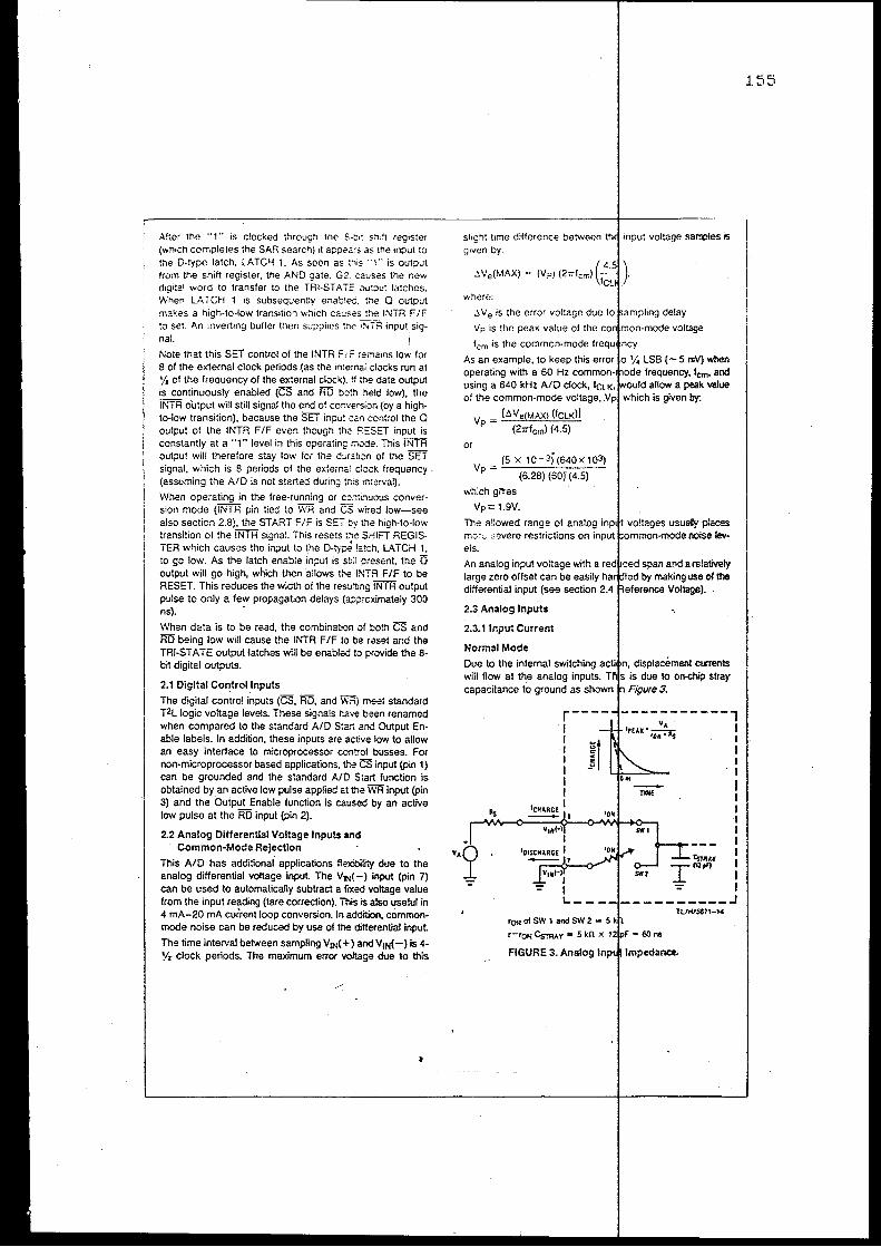
After the "'1" is clocked through the S~c~: sh:!l register (wh1ch completes the SAR search) it appeacs as tne .nput to the 0-type latch. LATCH 1. As soon as m1s .. , .. is output from the shift register, the AND gate. G2. causes the new d1oital word to transfer to the TRI-STATE ou:::>ut latches. When LATCH 1 is subsequently enable~. the 0 output makes a high-to-low transition which causes t~ INTR F/F to set. An inverting buffer then supplies t:->e ;:-, TR input, signal.
Note that this SET control of the INTR F;f' rema1ns low for 8 of the external clock periods (as the internal clocks run at 'Is of the frequency of the external clock). If the data output is continuously enabled (CS and RO both held low), the INTR output will still signal the end of conversion (by a highto-low transition), because the SET input can control the 0 output of the INTR F/F even though tr~ R:OSET input is constantly at a "1" level in this operating mvde. This INTR output will therefore stay low for the d~ration of the SET signal, which is 8 periods of the ex'terna! c:oc!< frequency . (assuming the AID is not started during t:\is interval).
When operating in the free-running or cc:1ti.1uous conversion mode (INTR pin tied to WR and CS wired low-see also section 2.8), the START F/F is SETty the high-to-low transition of the INTR signal. This resets t!'H? SHIFT REGISTER which causes the in;>ut to the 0-ty~ !atch. LATCH 1, to go low. As the latch enable input is stiil present, the 0 output will go high, which then allows the INTR F/F to be RESET. This reduces the width of the resulting INTR output pulse to only a few propagation delays (a;:>p;oximately 300 ns). ·
When data is to be read, the combination of both CS and RD being low will cause the INTR F/F to be raset and the TRI-STATE output latches will be enabled to provide the 8-bit digital outputs.
2.1 Digital Control Inputs
The digital control inputs (CS. RO, and Wi'i) meet standard T2L logic voltage leve!s. These signals ha~ been renamed when compared to the standard A/0 Stan and Output Enable labels. In addition, these inputs are active low to allow an easy interface to microprocessor control busses. For non-microprocessor based applications. the CS input (pin 1) can be grounded and the standard AID Start function is obtained by an active low pulse applied at the WR input (pin 3) and the Ouiput Enable function is caused by an active low pulse at the RO input (pin 2).
2.2 Analog Differential Voltage Inputs and Common-Mode Rejection
This AID has additional· applications flexibility due to the analog differential voltage input. The VJN(-) input (pin 7) can be used to automatically subtract a fiXed voltage value from the input reading (tare correction). This is also useful in 4 mA-20 mA current loop conversion. In addition, commonmode noise can be reduced by use of the differential input
The time interval between sampling YIN(+) and YtN(-) is 4-y~ clock periods. The maximum error YOI'.age due to this
slight t1me difference between given by:
where:
input voltage sa~tes Is
As an example, to keep this error LSB (- 5 mV) when operating with a 60 Hz coJnrrJon-rl11)de frequency, fern, and using a 640 kHz AID clock, allow a peak value of the common-mode voltage, which is given by:
or
Vp = [t.Ve(MA)O (fcLK)]
(211"fcml (4.5)
(5 X 1Q-3j (640X 103)
Vp = (6.28) (60)'(4.5)
which g~es
Vp""1.9V.
The allowed range of analog voltages usualy places mcc,_ ~evere restrictions on input t:omOTlDn•-mi)Oe noise levels.
An analog input voltage with a large zero offset can be easily differential input (see section 2.4 RP,fer·en,~e
2.3 Analog Inputs
2.3.1 Input Current
Normal Mode
Due to the internal switching will flow at the analog inputs. capacitance to ground as shown
r---- -----------, VA I 1
I ·I I I I I
lruK· •oo •lis I
I I I I I I I I I I I I I _________ .J
TL/KIS671-1"'
155
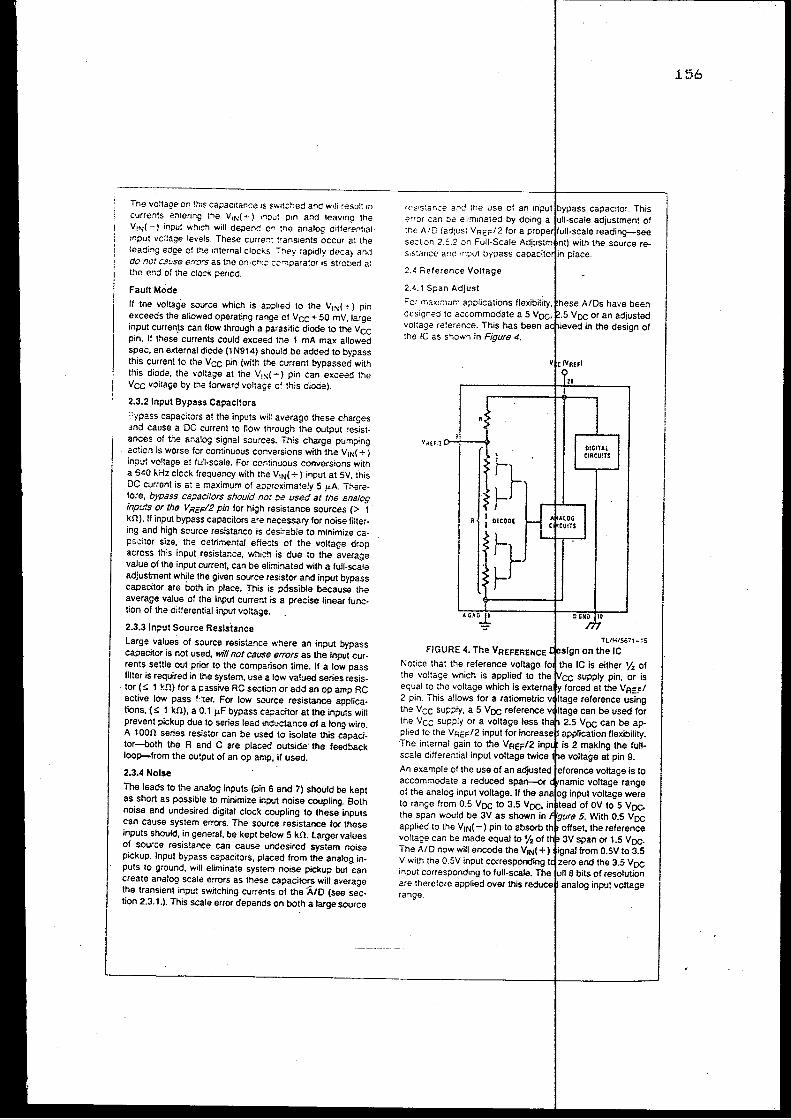
The voltage on th:s capacitance JS sw1t.:hed and wtJi result1n currents e~tenng the V1r .. :( ... ) t"'!O.;~ p1n and leavtng the V1N(-) input w~·uch will depend oc !'le analog di!fen?nttal 1nput voltage levels. These curre~~ !rar.sients occur a! the leading e.:lge o! the internal cloc•.s '7'ney rap1dly dec a;· and do no: Ca!J·se errors as t~e on-e~:~ :~mparator •s strobed at the end of the c:ock penod.
Fault Mode
If the voltage source which is apphed to the V1N(-+) p.n exceeds the allowed operatipg range of Vcc+50 mV,Iarge input curren!s can flow through a parasitic diode to the Vee pin. If these currents could exceed the 1 mA max allowed spec. an external diode {1 N914) should be added to bypass this current to the Vee pin (with the current bypassed with this diode, the voltage at the V1~( ~) pin can exceed the Vee voltage by the forward voltage cf this diode).
2.3.2 Input Bypass Capacitors
"ypass capacitors a! the inputs win average these charges Jnd cause a DC current to flow tn,ough the output resist· ances of the analog signal sources. This charge pumping action is worse for continuous cor.versions with the V~t.:( + ) input voltage at full-scale. For continuous conversions with a 640 ~.Hz clock frequency with the v,N( +) input at 5V, this DC current is at a maximum of approximately 5 !'A. Therefore, bypass capacitors should not be used at tne analog inputs or the VR;:Fi2 pin for high resistance sources{> 1 k!l). If input bypass capacitors are necessary for noise filtering and "high source resistance is desirable to minimize cap<;citor size, the detrimental efiec:s of the voltage drop across th;s input resistance, which is due to the average value of the input current, can be eliminated with a full-scale adjustment while the given source resistor and input bypass capacitor are both in place. This is possible because the average value of the input current is a precise linear function of the differential input voltage.
2.3.3 Input Source Resistance
Large values of source resistance where an input bypass capacitor is not used, will not cause errors as the input currents settle out prior to the comparison time. If a low pass filter is required in the system, use a low valued series resis· tor { ~ 1 k!l) for a passive RC section or add an op amp RC active low pass f':ter. For low source resistance applications, ( $ 1 k!l), a 0.1 f1F bypass ca;:acitor at the inputs will prevent pickup due to series lead inductance of a long wire. A 1 oon series resistor can be used to isolate this capaci· tor-both the R and C are placed outside· the feedback loop-from the output of an op amp, if used.
2.3.4 Noise
The leads to the analog inputs (pin 6 and 7) should be kept as short as possible to minimize input noise coupling. Both noise and undesired digital clock coupling to these inputs can cause system errors. The source resistance for these inputs should, in general, be kept below 5 k!l.largervalues of source resistance can cause undesired system noise pickup. Input bypass capacitors, placed from the analog inputs to ground. will eliminate system noise pickup but can create analog scale errors as these capacitors will average the transient input swilching currents of the AID (see section 2.3. 1.). This scale error depands on both a large source
res,stanc-e and the use of an mput error can be el!m•nated by doing a the A/D (ad;ust VqEF/2 for a nr.~o<>rlll'ull-sc:ale sect1on 2.5.2 on Full-Scale AOIUsimt!l SiStance ar1d mput bypass c"'oac:itorlin
2.4 Reference Voltage
2.4.1 Span Adjust
For ma.<imum applications flexibility, designed to accommodate a 5 Voc. voltaoe reference. This has been the IC as shown in Figure 4.
range.
156
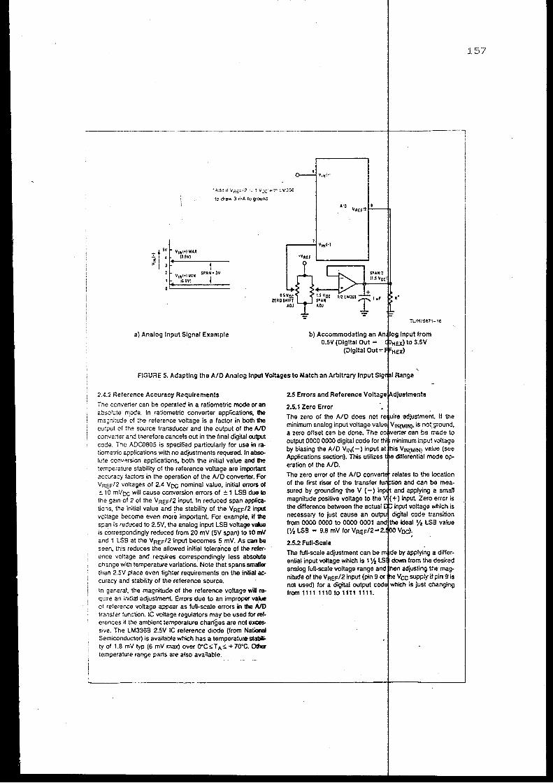
·Add 1t VrH::•'2 -_! v.x- ... ·!!'> :..\~356
to draw 3 MA to gouoa
- ' sv I v,.,., MAX ~I I !l5V) > I 3 +-----,1 --
z t SPA,. •lV V1NHMIN I 1 l0.5Yt 1
a) Analog Input Signal Example b) Accommodating an O.SV (Digital Out =
(Digital Out=
F!GURE 5. Adapting the A/0 Analog ln.,ut Voltages to Match an Arbitrary Input
2.4.2 Reference Accuracy Requirements
The conver1er can be operated in a ratiometric mode or an a::solute f11ode. In ratiometric converter applications. the ma"ni:ude of the reference voltage is a factor in bo1h the output of the SO!.Jrce transducer and the output of the AID converler and therefore cancels out in the final digital output code. The ADC0805 is specified particularly tor use in ra- · tiome:ric ajJplications with no adjustments required. In absolute conv-.rsion applications, both the initial value and the temperature stability of the reference voltage are important accuracy factors in the operation of the AID converter. For YREF/2 voltages of 2.4 Yoc nominal value, initial errors of :::10 mVoc will cause conversion errors of ± 1 LSB due to the gain of 2 of the Y REF/2 input In reduced span applications, the initial value and !he stability of the VREF/2 input voltage become even more important For example, if the span is reduced to 2.5'1, the analog input LSB voltage value is correspondingly reduced from 20 mV (5V span) to 10 mV and 1 LSB at the VREF/2 input becomes 5 mV. As can be seen, this reduces the allowed initial tolerance of the reference voltage and requires correspondingly less absolute change with temperature variations. Note that spans smaRer than 2.5Y place even tighter requirements on the initial accuracy and stability of the reference source.
In general. the magnitude ol the reference voltage wilt r&
quire an initial adjustment Errors due to an improper value ot reterence voltage awear as tun-scale errors in the ivo transfer function. IC voltage regulators may be used for references it the ambient temperature changes are not excessive. The LM3368 2.5V IC reference diode (from Nationat Semiconductor) is available which has a temperature~ ty of 1.8 mY typ (6 mY max) over o·c,;; T A,;; + 70"C. Other temperature range parts are also available.
2.5.1 Zero Error
The zero of the A/D does not minimum analog input voltage a ZE!!'O offset can be done. The output 0000 0000 digital code for by biasing the AID YtN(-) input Applications section). This utilizes eration of the AID. The zero error of the A/0 of the first riser of the transfer sured by grounding the V (-) magnitude positive voltage to the the difference between the actual necessary to just cause an from 0000 0000 to 0000 0001 ('/2 LSB = 9.8 mV for YREF/2=
2.5.2 Full-Scale
The full-scale adjustment can be entiat input voltage which is 1 Y2 analog full-scale voltage range nitude of the VReF/2 input (pin not used) for a digital output from 1111 1110 to 11111111.
TL/H/5671-16
is not:ground. be r..ade to
and can be mea-applying a small
) input. Zero error is voltage which is code transition
ideal Yz LSB value Voc).
by applying a differfrom the desired
adjusting tl"~ magVee supply if pin 9 is
which is just changing
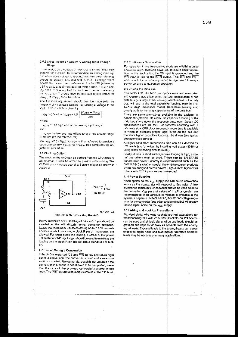
2.5.3 Adjusting tor an Arbitrary Analog Input Voltage Range
It the ar.alcg :e0 voltage of the AID is shttted away frc;n ground (for exa-r.;:>ie. to a:commodate an analog .nput s1g· :,._-:; · whiCh dces no! go to ground} thiS new zero reference s~ould be :Jr(':)€~ly adJu:S!ed first. A V:N{- ) voltage whtch equals tn:s aes·!"ed zero reference plus 1
; 2 LSS (where tt'le LSS 1s calc ..J:a:e: for the destred analog span. 1 LSB = a0a· log s;,1an "2561 rs applied to pin 6 and the zero reference voltage a: p:n 7 s~o":fld then be adjusted 10 just Ot'tain tne OOHE\ to 01,..:;x code transition.
The lull-scale adjustment should then be made (with the proper ViN(-) voltage applied) by forcing a vo!iage to the VIN(-) input which is given by:
, .. [ (VMAX- VM!N)] v,N(-J.saCj=VMAx-1.5 256
•
where:
VM.;x = T;,e high end of tne analog input range
and
V1."'J = t:;e low end (the otiset zero) of the analog range. (Both are ground referenced.)
The VR::Fi2 (or Vee) voltage is then adjusted to provide a cod.: change f:-om FEHEX to FFHEX· This completes the adjustment p:-ocedure.
2.6 Clocking Option
The clock for the AID can be derived from the CPU clock or an external RC can be added to provide self-clocking. The CLK.IN (pin 4) makes use of a Schmitt trigger as shown in Figura 6.
ClJ: A
" 1 !eLK"' 1.1 RC
R"'10 kO
A/0
TLIH/5671-17
FIGURE 6. Self-Clocking the A/D
Heavy capacitive or DC loading of the clock R pin should be avoided as this will disturb normal converter operation. Loads less than 50 pF, such as driving up to 7 AID converter clock inputs from a single .clock R pin of 1 converter, are allowed. For larger clock line loading, a CMOS or low power T2L buffer or PNP input logic should be used to minimize the loading on the clock R pin (do not use a standard T2L buffer).
2.7 Restart During a Conversion
If the AID is restarted (CS and WR go low and return high) during a conversion. the converter is reset and a new conversiofl is started. The output data latch is not updated if·the convers.on in process is not allowed to be completed, therefore the data of the previous conversioi\: remains in this latch. The INTR output also simple remains at the "1"1evet
2.8 Continuous Conversions
For operat,on in the free-running should oe u~ed. following oower-u'"· t1on. In this application, the WR input is tied to the node should be .momentarily
will reqUtre a bus driver data bus gets large. Other bus, will add to the total ca,pa!:1111re STATE (high impedance
an initializing pulse insure circuit opera
is grounded and the This WR .and INTR
greatly adds to the stray '"""'"cit;ort'·" There are some lnRrm'""'"' handle this problem. data bus slows down specifications are still
to the designer to
""""'"·'"•" loading of the even though DC operating with a time is available on the bus and
relative I}' slow CPU clock rrenuen.nllf in which to establish proper therefore higher capacitive loads be driven (see typical characteristics curves).
At higher CPU clock frequencies 1/0 reads (and/or writes) by using clock extending circuits
Finally, if time is short and ""~-'""'""'" nar bus drivers must be used. buffers (low power Schottky is re<lnn,m,emled such as the DM74LS240 series) or special which are designed as bus drivers with PNP inputs are re<:orndhende<d.
2.1 o Power Supplies
system, a separate Lr<I.>'>VL~<£.-;> .. u,l
later for the converter (and reduce digital noise on the Vee
can cause conversion · to this noise. A low
should be used close to of 1 p.F or greater are
is available in the SV voltage regu-
circuitry) will greatly
2.11 Wiring and Hook-Up "''"'""''""''"" Standard digital wire wrap breadboarding this AID can be used and all logic grouped and kept as far away signal leads. Exposed leads !O undesired digital noise and hum leads may be necessary in many aJ>plic:ations.
158
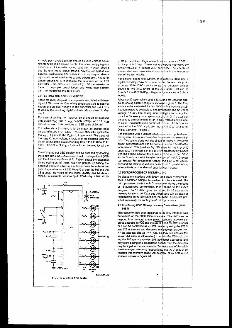
A s1ngle po1nt analog ground should be usee v.hich is separate from the log1c ground PO•'lts. The powe' supply bypass capacitor and the self-ciock1na capac1tor t•l used) should both be returned to d•gital groCnd. Any V;;::/2 bypass capacitors, analo.g input filter capacitors, or mput s•gnal shieldmg should be returned to the analog ground po1nt. A test for proper ground1ng is to measure the zero error of the AID converter. Zero errors on excess of ',;~ LSB can usually be traced to improper board layout and w~ring (see section 2.5.1 for measunng the zero error). ·
3.0 TESTING THE AID CONVERTER .
There are many degrees of complexity associated with testing an AID converter. One of the simplest tests is to apply a known analog input voltage to the converter and use LEOs to display the resulting digital output code as shown in Figure 7.
Fbr ease of testing. the VREF/2 (pin 9) should be supplied with 2.560 Voc and a Vee supply voltage of 5.12 Voc should be used. This provides an LSS value of 20 mV.
If a full-scale adjustment is to be made, an analog input voltage of 5.090 Voc (5.120-1% LSB) should be applied to the VIN( +) pin with the V1N(-} pin grounded. The value of the VREF/2 input voltage should then be adjusted until the digital output code is just changing from 1111.1110 to 1111 1111. This value of VREF/2 should then be used for all the tests.
The digital output LED display can be decoded by dividing the 8 bits into 2 hex characters, the 4 most signifiCant (MS) and the 4 least significant (LS). Table I shows the fractional binary equivalent of these two 4-bit groups. By adding the decodad volta.;es which are obtained from the column: Input voltage value for a 2.560 VREF/2 of beth the MS and the LS groups, the value of the digital display can be determined. For example, for an outp:Jt LED display of1011 0110
tOt
svoc
''11./H/5671-18
HGURE 7. Basic AID Tester
or 86 (in hex). the voltage values 0 120 or 3.640 Voc These ce,-,ter -values of a pertect quaf1,t1Zation error have to be accour.::<1c
tion of the test results.
For -a higher speed test system. or to d•gital-to-ana!og converter 1s needed accurate 1 O-bit DAC can serve as source for the AI D. Errors of the provided as etther analog voltages or "'"""''n''"'" words.
A basic AID tester which uses a DAC as an analog output voltage is amps can be elminated if a lab DVM traction feature is available to directly voltage, "A-C". The analog input by a low frequency ramp nAon"''""" be used to provide analog error (X axis). The construction details provided in the NSC application Digital Converter Testing".
For operation with a microprocessor test system, it is more convenient to t,,•·i- This can be done with the output code transitions can be incremented. This provides y. under tesllf t'le results of this tr:s: with the analog input on the X axis as the Y axis, a useful transfer test results. For acceptance
. sary and the testing sp;ed can be internal limits on the allowed error
4.0 MICROPROCESSOR INTERF A
To dicuss t'le interface with 6080A sors, a common sample subroutine microprocessor starts the AID, re<;~ds of 16 successive conversions, then program. The 16 data bytes are memory lcr...ations. All Data and Annr•·""''" hexadecimal form. Software and vided separately for each type of mi<,rhr>r"'"'"'''"'
4.1 lnterfacing.SOBO Mlc:rot>ro•~es.so~ 8085)
mapped into·memory space '~i§~l~r'd dress decoding for CS and the or it can be controlled as an 1/0 and 110 W strobes and decoding the A7 (or address bits AS -+ A15 as same 8-bit address information) to nhlll:>ir• '"'"
ing the 110 space provides 256 may allow a simpler 8-bit only be input to the accumulator. tiona! memo<y reference im:tmMi<'""
mapped into memory space. An space is shown in Figure 10.
159
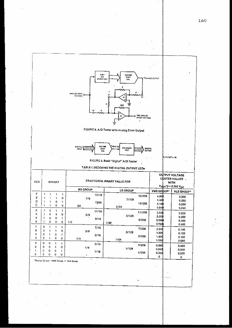
HEX BINARY
F 1 1 E 1 0 0 0 1 c 0 0
B 0 1 A 0 ,1- 0 9 0 0 1
_8 0 0 0
7 0 1 6 0 1 0 5 0 0 1 4 0 0 0
3 {) 0 1 1 2 0 0 1 0 1 0 0 0 1 0 0 0 0 0
A'-AlOG liliPUT VOL TAC£
OIGJTAL 1'-'UT
-c-
-.-
FIGURE 8. A/0 Tester wi!h Analog Error Output
AID UNDER DIGITAL TEST OUT,UT
FIGURE 9. Basic "Digital" A/0 Tester
T ~BLE I. DECODING THE DIGITAL OUTPUT LEOs
FRACTIONAL BINARY VALUE FOR
15/16 718 7/128
1:f'16 13/256 4/4 3/64
11/16 11/256 5/8 5/128
9/16 9/256 1/2 1/32
7/16 7/256 3/8 3/128
5/16 2/256 1/4 1/64
3/16 3/256 1/8 1/128
1/16 1/256
"Disp•ay Q::M =VMS Group + VLS Group
160
0.280 0.260 0.240
0.220 0.200 0.180 0.160
0.140 0.120 0.100 0.080
0.060 0.040 0.020
0
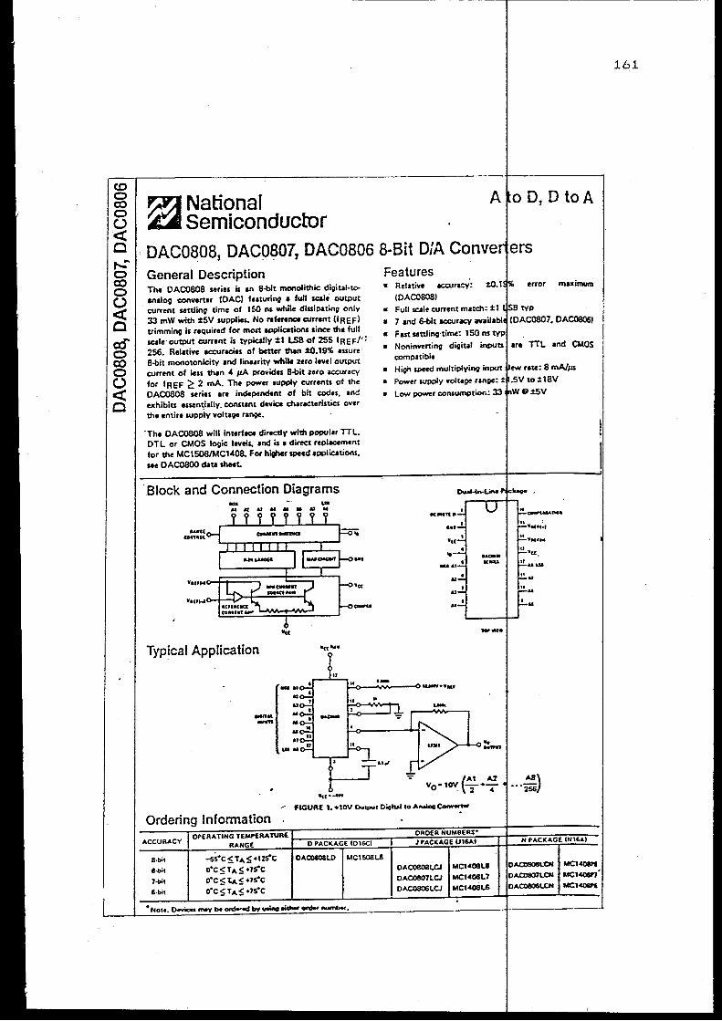
co 0 co 0 (.,) <! c
"' 0 co 0 (.,) <! c aS 0 co 0 C) <! c
~National ~Semiconductor
DAC0808, DAC0807, DAC0806 8-Bit DiA General Description Features The· OAC0808 series is an 8-bit monolithic digital·to- • Relative analog convener (OACI featuring a full scali output c:urrent settling time of 150 ns wht1e dissipating only 33 mW with ±5V supplies. No reference current (I REF I trimming is required for most applications since the full scale· outPUt current is typically ±1 LSB of 255 IREFI':· 256. Relative acc:uraeies of better than ±0.19% assure· 8-bit monotonicity and linearity while zero level output c:urrent of less than 4 pA provides 8-bit zero accuracy for IRE F 2:: 2 mA. The power supply currents of the OACOSOS series are independent of bit codes, and • Low power consumption: 33 exhibits essen~ally_ constant davie& c:har.cteristics over the entire supply voltage range.
"The OACOS08 will interfaee directly with POPUlar TTL, DTL or CMOS logic levels, and is a direct replacement for the MC1508/MC1408. For higher spHd applications. see OACOBOO data sheet.
·Block and Connection Diagrams
•u
Typical Application --·
....... ,-; I
..... j.::.<>--...,.. ...... --o ,._. .....
...... .. .. •• ....
L-...,...---1
.. ..
(At A7
Vo•10V -+. 2 4
FIGURE 1. +10V Ou-t Oloiulto ANiot eo.w-
Ordering Information
OAC0808LCJ MC1408U
OAC0807LCJ MC1408L7 OAC0806LCJ MC1408L6
161
error maximum
... ;:)
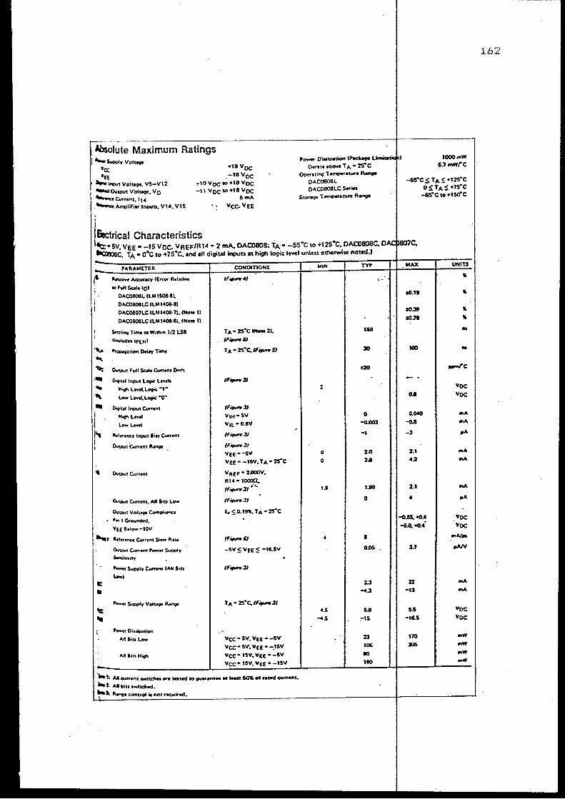
Absolute Maximum Ratings .._ Suc»ly Voltage
•a: •n
..... I"'>Jt Voltage, V5-V12 ~ Ovu>vt Voltage, Vo ~Currtnt,lt4
. ~Amplifier lnQUU, V14, VIS
' I
+tsvoc _-tsvoc
.,-to voc.., +tB voc -11 voc"' +tB voc
f>mA
Pow« Oissic>etion II'Kbpe Liooia1tiOI>l Oentt abOW TA • 25"C
()peralin; Temporat"" Range
OACOSOSL OACOSOSLC SarMI
St~ Temparaturt R-
IOOOmW 6.lrnWfC
-65"C !> TA $ +t25"C O$TAS+75"C
-65"C to +150" C
IEtctrical Characteristics Itt:;. sv. Vee- -15 Voc. VREFIR14- 2 mA. OAC0808: TA• -ss·c to +125"C. OAC0808C. DA~lJl'SQ/\;. ~c. TA • o•c to +7s•c. 1nd 111 digital inputs 11 high logic level unless otherwise noted.!
~ .. ,..., IV::t:»rKY fEnor Rclati"
10 full Scole tol
0AC0808LILM1~8L
0AC0808LC ILMI408-81
0AC0807LC ILMI408·71.1Nott11
0AC0806LC ILM1408-lii.INote II
Sn11inv Tirnt to Within 112 LS8
II"CludfltpLHI
'11;. l'roo•v .. ion Delay Tjme
~
'lit: CNtout full Scole Currtnt Otilt -.. " .. I ~lot I I
O.,t111 Input LoPe Lntll
HivJ> Lt¥tl Lev< •1•
Low Lntllov< -o• o;,;111 Input Curront
HivJ>Lntl
Lowlntl
Atfttenee Input liu Curre-nt
Ovtout Current Rant<
~tCurrent
OuUJut Cutttnt. All Bits low
Ov....,t Voltogc Cornolianct
"'-' I Grounded.
Y££ lelow-tOV
...,., Adercnco Currtnt Slew ""'
Owtwt Cun.nt Power SYP91y
s.,..;, .. i,.
'-Supply Curront fAll Btts
"-I
~ DilliPttion
Al1 Biu Low
All Bttl HivJ>
IF..,.41
TA•lS"C-21. ,,..,.SJ TA•25"C.fF.,_$/
,..,.31
VJH•5V
VtL •O.BV
IF;gu,.31
tF;gu,.3J
vee-~v
VEE • -15V. TA • 25"C
VREF • 2.000V. Rl4•tooon. (F..,.31<:.._
(F;gu,.3/
E,~O.t~ T.i•25"C
(F;gu,.Q
-5V ~ VE[ S -16..5V
Vee • SV. V[[ • -5V
Vee• 5V. VEE • -.15V
Vee • ISV. V££ • -!IV
Vee • 15V. V££ • -t5V
.... I; AJI current IW'itdwt •• '"'ed to.,.,.,...,_ M t.est ~ ol rated culftnL
... l AllbitsowltcMcl •
.... k 1\onve control ;. ""' requirod.
0
0
u
4.5
-4.5
150
30
0 -o.ool
-I
2.0 2.0
1..19
0
I
o.os
:u -4.3
5.0
:-15
33 106
to Ito
~-"
100
0.8
0.040
-o..tl
-3
u •.2
2.1
• -o.55.+0.4 -5.0..+0.4
2.7
22 -13
5.5
-16.5
no l05
• ..
"'"' ......
voc voc
... w
... w
... w -
162
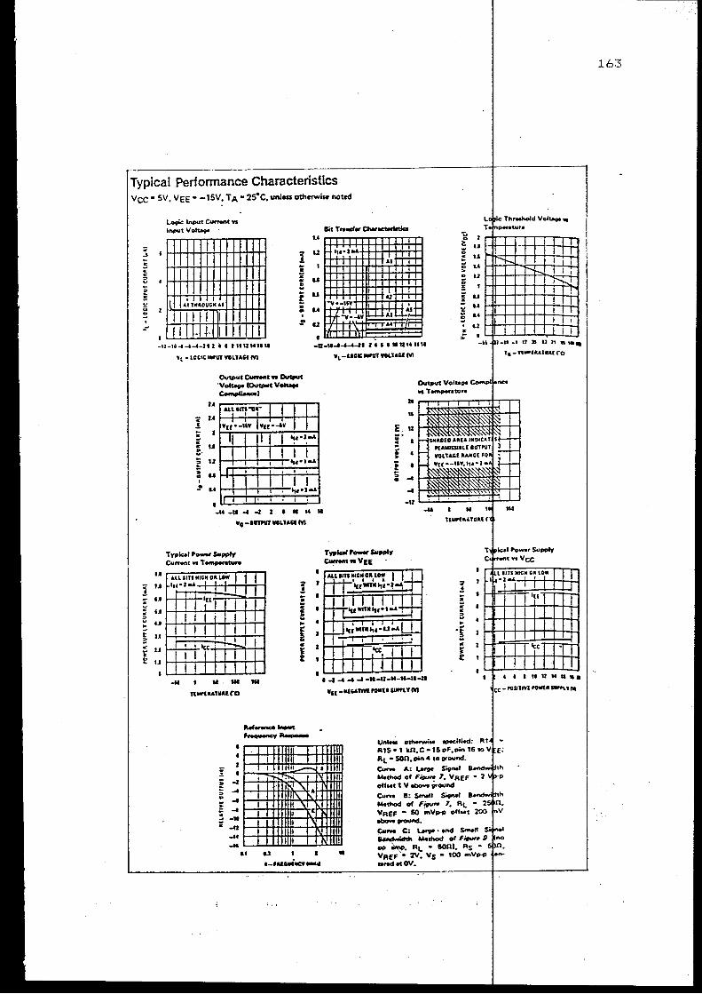
Typical Performance Characteristics Vee • sv. VEE • -t5V, TA • 2s"C, unlea otherwise noted
.. .. c .. ... .. .. ... ~ '
.:'
< .! . "' " e .. t a c
" f
II II II II
ll ~.~ 1M~OUG~ AI
IIIII 111 1111-lllll I
.. ~ t.J > u Hlr-+-''t--oC:---1--!-+-.l-W .. u Hll-+-+-++::::;...~L.;....!.J .. = ! u .. u Hll-+-+-+-+-+--L--!-!.J ; t.t Hi!-+-+-+-+-+-+-.!-~ . z >
·11-11-1 4-'-Zil I I IIIII Mllll -U-11~4-'-11 l• I I 11UM 1&11
u
1.1
u
1.1 ... u
2.1
IJ
Yt- LOGtttorUT VOUAGIM WL -UGICIWIIIVOUACIM
Output c-o ... Oucpuc ·v""- COonput v.._ Output Vol- c;o. .. p~jo .. .,. ~, w T..,.._"•tu••
u
~ u :~~OJ AL~II~-or I I I I .! vu•-11¥ vu·~w I I .. " " " u ;;. .. u :: " u 0 . ~ u
I II I I .... , ... I I I I I .... , ...
I ' ' ' ' I I I I I
I .... 1 ...
I . ' I
-M ·11 ~ -l Z I II M II
Vo ·IVUVT VOLlloCl M
ALLIITI MIGM OIILOW I .,., .... ' I
I i ~ti I I I I i I I I I I I I
+ttri ..... I I I
" w
" " e .. ·t ;:
c
" f
I I I I I ~~~~~~--._~~ I -l -1 -1 -1 -11-U -M-11-11-11 U 1M HI
f(W(U.lllll(Q
1111 I I 1111111 I -1
- • ~
-l .. .... 0
-1 w
~ -1
I ~~~---- I I
.. , I
. '' ~~ I '\I
c ~ -11 . -a I _ .. ... I ...
1 ••
¥1(-IIC&Anvl-I&IMI.YM
lfl m II
..
u- ott-wtM _.:itl.d: R15•1kn.C•15pf,pin1610 RL • son. pin 4 to •ound.
eu.- A: ~ Si9-l Method of F;g,n 1'. VREF • 2 ofl,.t1 V ebovo jround
Cune 8: SINII Sionof ~ of Fipu,. 1. RL • VREF • &0 mVrHJ oftHt 200 ebovo..-ncf • Curwe C: .... ._. • ond Small ~ t.lfthocl otF;,.op ~. RL • &ani. Rs • VREF • 2V. Vs • 100 mVrHJ ttredatOV.
t I IIIUMII•a
- PCSZliVI rowta """'-"~f'l
1.63
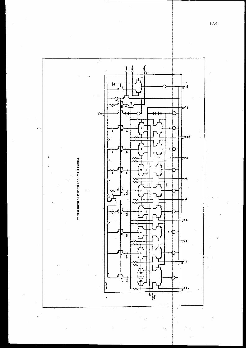
l 0
i r r
1.64
. !
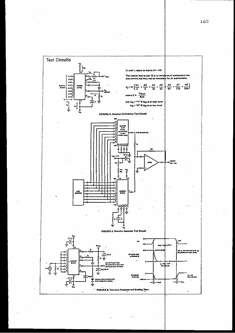
Test Circuits
........ I~ ....,. .. .. .. .. .,_
Ytond It -'Y to Inputs A1-A8 •
Tho rniotor tiod to pift 16 i& to,..,...,.,.,,..,..~,.,... bios ........,,ond mav not bo fot au a;>C>Iicotion&.
(A1 Al A<l AS
lo•K 2+4+16+32
-.K• VREF R1<l
:1 ~·t~ -...,- •t" If..., Is rt high
...,- "V' If,.., ••• --...
. .. FIGURE .C. R.Utlvo "'-w:r Toot Circuit
"a:
-.... .. .... .. _ .. -. "••m•ct• .. :.~.-:= :::.:: ...
~ .. ~ ... ... - ..... - .... " .. I ......... PHCtfMCI.. -= ....... Q'If'l.'f.....U
... • PICURE IL T..w-t R--s...-..T-
165
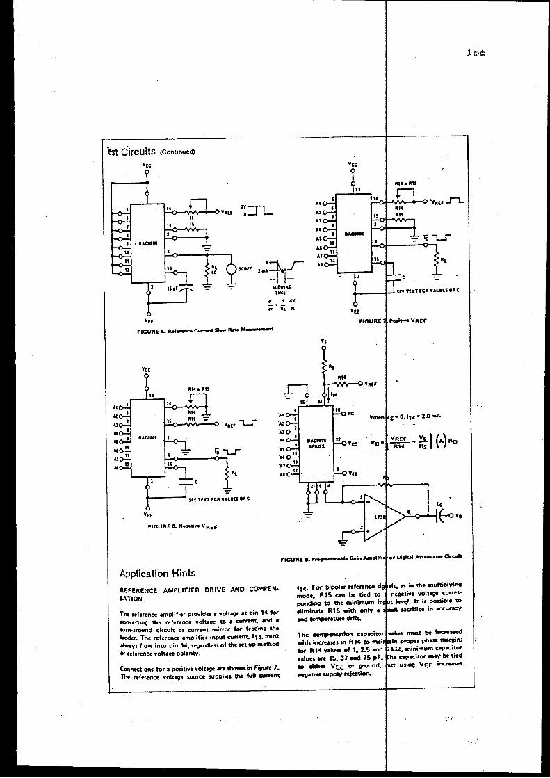
tst Circuits (Contonued)
lt
&:
&.1
iiC
• II
&.1
II
• DAC1llt
SUWI., liM{
• 1 IV ;;·iL ..
FIGURE 6. R.f.nnce Oment Q.- Rate M.-;~reftMnt
Yet
t Rl4•1115
AI
-vau "1-r ·.u Al ..
tO ""L..r AS .,., .,.,
~ ... -=
SU TUT fOAVAUlSOfC
vu
FIGURE 8. N-t;,o V REF
Application Hints
REFERENCE AMPLIFIER DRIVE AND COMPENU.TION
The reference omplifier provides a "oltage at pin 1• tot COoverting tho reference voiUQO to a curr.nt. and a !Urn-around circuit or current mirror tor feed"'9 the &.dder. The reference amplifier input current. 114· tnutl
always flow into pin 14, regardless of the set-up method O< reference voltage polarity.
Connections for a positive voltage are shown in Fiyrlrr 1. The reference voltage source suppliu the fvD current
Vee
Wl\on • O.lt• • 2.0 fftA
~.~) (~.)Ro Vo • R14 . Rs
114· for bipolor reference mode. R15 can be tied pending to the minimum .timinate R 1 S with only a and wemperature drift.
The compensation copacitor with increHH in R14 to tor R 1• nlues of 1, 2.5 and values are 15. 37 and 75 pF. to either vee or ground, IIOIPtW• supply rejection.
value must be increased proper phase marvin:
minimum capacitor capacitor may be tied using Vee inc:re~
l.66
Application Hints IContinuedJ
A neQative referena voiUQ< m.y be used if R14 is. grounded and the referenct voluqe is applied to R 15 as .. shown in Figure 8. A hi9h input impedance is the main advantage of this method. Compensation involves 1 c:.~padtor to Vee on pin 16. using :ne values of the previous ptragraph. The negative reference voluge must be at least 4V above the VEE supply. BiPOlar input signols may be handled by connecting R14 to a positive reference voltage eQual to the pealt positive input level
npin 15.
When a DC reference voltage is u~. a;~~Citive bypass to ground is recommended. The SV logic supply is not recommended as a reference 'voltage. If 1 well regulated 5V supply which drives logic is -to be used as the refer· ence. R 14 should be decoupled by connecting it to SV through 1nother resistor and bypassing the junction of the 2 resistors with 0.1 pF to ground. For reference voltages greater than SV. a damp diode is recommended between pin _14 and ground.
If pin 14 is driven by a high impedance such as 1 transistor current source. none of the above compe,.. tion methods apply and the amplif .. r must be huvily compensated. decreasing the overall bandwidth.
OUTPUT VOLTAGE RANGE
The voltage on pin 4 is restricted to a range of -0.6 to O.SV when Vee • -5V due to the current switd'oing methods employed in the OAC0808.
The negative output voltage compliance of the OACOSOS is extended to -SV where the negative supply voltage.is more negative than -10V. Using 1 full-scale current of 1.992 mA and load resistor of 2.5 k!l between pin 4 and ground will yield a voluqe outpUt of 256 levals between 0 and -4.980V. Floating pin 1 cioes not affect the converter speed or powef" dissipation. However. the value of the load resistor determines the switching time due to increased voltage· swing. Vai<Hs of Rt up to soon do not significantly affect perfomunc:e. but • 2.5 k.."l load increases worst-ase settling time to 1.2 ps (when all bits are switd'oed ON). Refer to the subseQuent text section on· Settling Time tor more details on oulPUt loading.
OUTPUT CURRENT RANGE
The outP<Jt current maximum rating of 4.2 mA may be used only for negative supply voltages more neptive thin -7V. due to the increased .. otUge drop acrou the resistors in the reference current amplifier.
ACCURACY
of the monolithic resistor may drift with teone<rratur4. absolute ..:curacy of OACOSOB has 1 very low temperature.
This corresponds to a drive to the ladder 1 LSB (8 pAl which is the
Two 8-bit O·to-A constNCt I 16-bil
than the OACOSOB.
The referenca cunorc c:.~using a change in w..
current. However • .,. current drift wilo
used '10 converter.
1 1~
of ~1/2 of one Part;. much more ICXUrft
provided by .,.
in the multiplying lftOISt reference current il n•;.,
reference current in .,. 16 pA to 4 mA. w..
COiftVIIDUtK>IIIS lfe leSS than 1.6 pA. The when referred to full-laol&.
SETTLING TIME
which supplies an mc:r... in the binary ""01'4
11!"0<\()tOniC for all valua e1 mA. The recomii\Ofl(\od.
reference current is O.S '10
The wont-ease switd'oing occun when • biu are switd'oed ON. which toorres:oonds to a low·~ transition for all bits. time is typically 150 ,. for settling to within LSB. for 8-bit acanq. and 100 ns to 1/2 LSB 7 1nd 6-bit accuracy. Tht turn OFF is typically 100 ns. These times ICl9i'f when RL~soonandCo~ pF.
' board layout ainca !his ~ usually the dominant in satisfactoy ten ...wa when measuring settling Short leads. 100 ,.F supply bypassing for low freQuotncits. and minimon ecope lead length are all ..... ....tu~,rv.
167
Absolute accuracy is the measure of oacn output current level with respect to iu intended •alue. and is dependent upon relative accuracy and tub-scale current drift. Relotive accuracy is. the measun of e~ outP<Jt current lr~el as a fraction of the full-sale curnnt. The reutivt accuracy of the OAC0808 is essentially constant with temperature due to the excellent temperature tracking
~~-----------------------------~------------~
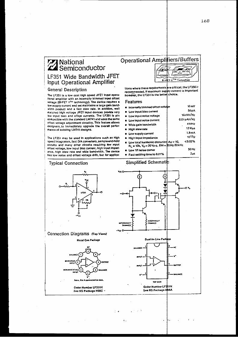
~National ~ Semiconductor LF351 Wide Bandwidth JFET Input Operational Amplifier General Description The LF351 Is a low cost high speed JFET Input opera· Uonal amplifier with an Internally trimmed Input oftset \'Oitage (BI·FET II"' technology). The device requires a low supply current and yet maintains a large gain band· width product and a last slew rate. In addition. well malched high voltage JFET Input devices pr<Mde very low Input bias and ollset currents. The LF351 Is pin compatible with the standard LM741 and uses the same offset voltage adjustment circuitry. This feature allows designers ,to Immediately upgrade the overall perter· mance of existing LM741 designs.
The LF351 may be used In applications such as high speed integrators, fast 0/A converters. sample-and.f\old circuits and many other circuits requiring low input offset voltage, low input bias current. high Input lrnped· ance, high slew rate and wtde bandwidth. Tile device has low noise and offset voltage drift, but lor applies·
Typical Connection
lions where these requirements recommended. II maximum however. the LF351ts the
Features • lnternallytrlmmedotlset
• Low Input bias current
• Low Input noise voltage
• Low Input noise current
• Wide gain bandwidth
• High slew rate
• low supply current
• High Input Impedance
• low 11f noise comer
• Fast settling time to 0.01%
Simplified Schemat
tOmV
50pA
16nVNHz
O.otpMfHz
4MHz
13VI,..s
1.8mA to12Q
.v,,o----~~-------+------------~~------~ Connection Diagrams CTop Viewsl
r Not•. l'iA ol ~ 10 UN ..
Order Number LF351H See NS Package H08C •
1.68
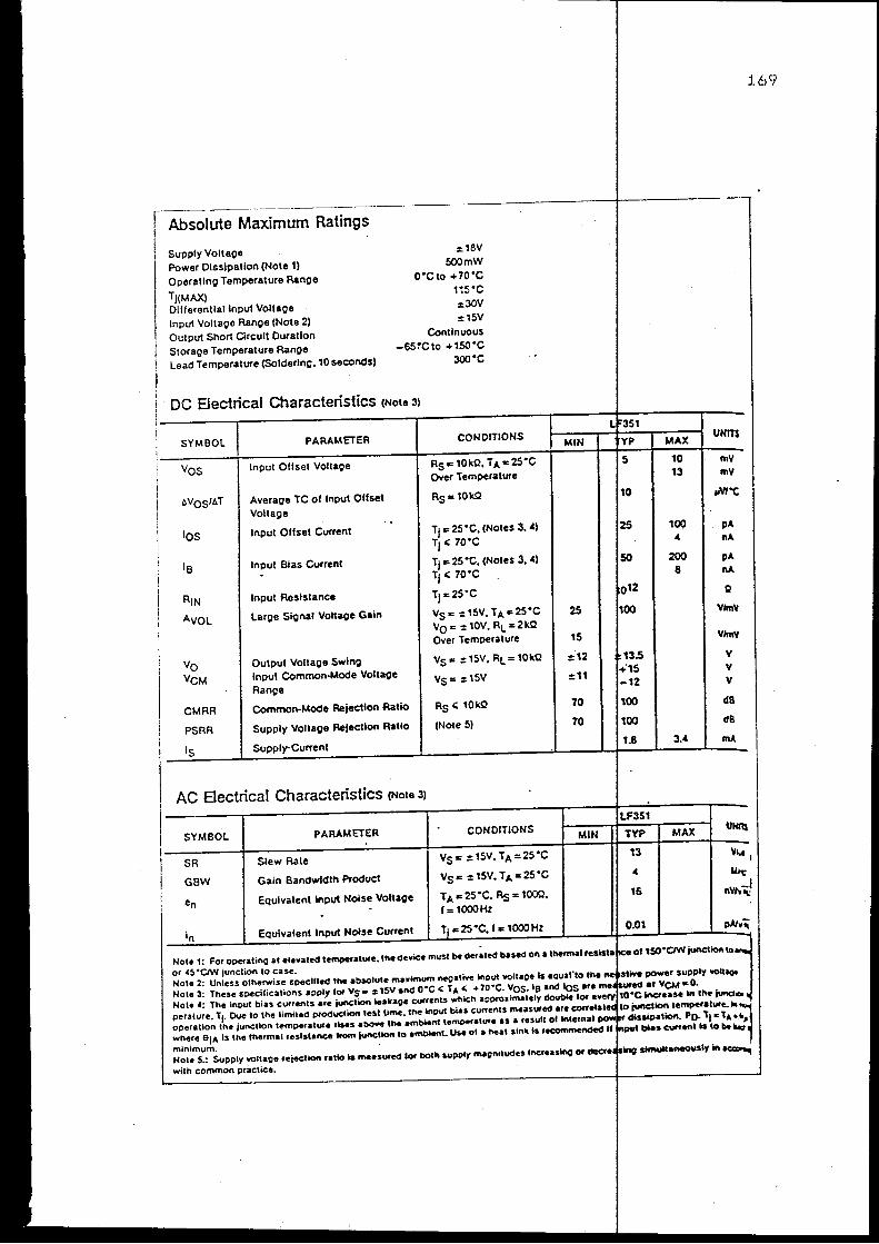
Absolute Maximum Ratings
Supply Volta9e Power Dissipation (Note 1) Operating Temperature Range
TJ(MAX) Differential Input Vollage Input Voltage Range (Note 2) Output Short Circuit Duration Storage Temperature Range Lead Temperature (Soldering. 10 seconds)
:18V 500mW
O"Cto +70"C 1~s·c
:30V :15V
Continuous -65~Cto +150"C
300"C
DC Bectrlcal Characteristics (Note 31
SYMBOL PARAMETER CONDITIONS
vos Input Oflset Voltage Rs"' 10kQ, TAo: 25"C Over Temperature
t.Vos'"'T Average TC of Input Offset Rso:10kQ
Voltage
•os Input Offset Current T; = 25 ·c. (Notes 3. 41 TJ < 70"C
Is Input Bias Current T; = 25 ·c. (Notes 3. 4)
Tj < 70"C
R1N Input Resistance Tjzi25"C
AvoL Large Signal Voltage Gain Vs o: :: 15V, TA c 25•C Yo c :: 10V. RL = 2kQ Over Temperature
vo Output Voltage Swing Vs= ::15V. RL=10kQ
VcM Input Common-Mode Voltage Vs= :15V Range
CMRR Common-Mode flejectlon Ratio Rs < tOkQ
PSRR Supply Voltage Rejection Ratio (Note 5)
Is Supply-Current
AC Sectrlcal Characteristics (Note 3)
25
15
i12
::11
70
70
10
25
50
100
100
1.8
10Q 4
200 8
3.4
UN In
mY mY
0
V/mV
V/mY
v v v
dB
dB
mA
1.69
13 y,_. I
4 lot~
16 v -1 II lv'l,:
0.01 pAt~~
Note 1: For operating at elevated temperature. the device ""'st be derated based on a tt>etmat res>istallo:e oi150•CIW junction to
or •5 'CIW junction to case. Note 2: Unless otherwise specified the absolute muimum negative input voltage is equarto the power supply ooltago Note 3: These specilications apply tor Vs • ::15V and o·c < TA < + 70"C. Vos.•a and tos are at VCM aO. Note •: The input bias currents are junction leakage currents whiCh approximately double tor ........ .,11n•r- inctease In the junao perature. T;. Due to the limited production test time. the input bias cunents measured are temperature ... operation the junction temperature rises abo.., the ambient temperature as a result of Internal Po- Tj "'tA where 6jA Is the thermal resistance kom tunctton to ambient. Use ot a heat sin~ Is recomrnended if bias current Is to be lr.ocr
minimum. Note 5.: Supply ooltage rejection ratio Is measured lor both supply mavnitudes Increasing or _,,.., .. ;r.., slmUit-ly in~ with common practice.
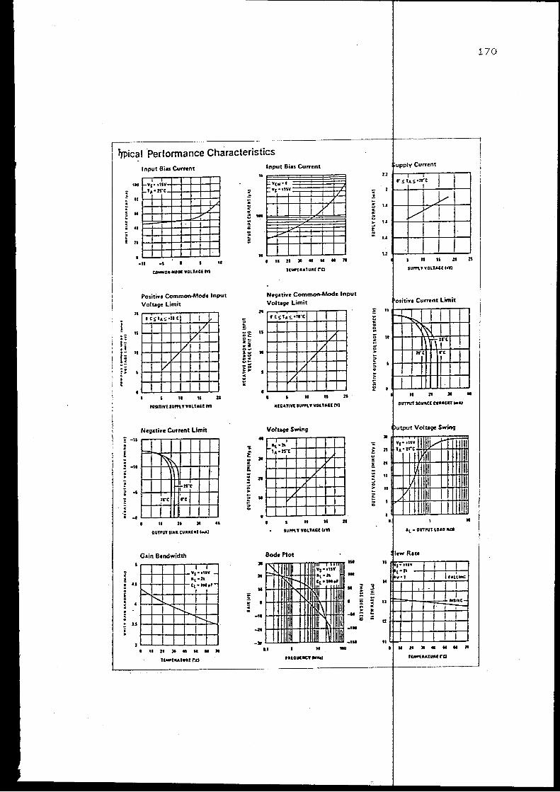
Typical Performance Characteristics
j . . . ~ <
~
:E 1: • ! ·-1: ·: .. ~· i
E . . l . ! . . E : . < . ·-.
1 ! . i : . : . i a
Input Bias Cunent
'" t-Vs• .uv 1-'•. n-t
" .. !..---
•• t--
I n I
I • ·II
_, "
Jt
II
II
I
-u
-II
...
...
t.l
l.S
COMMON-MOD( YOlTACl M
Positive Common-Mode Input Voltave Limit
I t~T·~·ll C I j ~
l I -, -JZ I I 171
VI ! v I
v
I • II
rosmvl sum. Y volt&el m
Negative Current Limit
1-. I ~
I I !Ln·c
' ll"t rc
I I .. ,. •• OUTPUT Sill CURAllfT t-.ll
Gain Bandwidth
'
.; .. J. -"" •h Ct•IM,,-·,
['.. I I I I" I
1' I T
II II :It 41 M II J1
UMrtAATUAl f".Q
~ . c
" ;: .. ,. "'
~ C:E o_
~! ,._ :IU ., .. .. --J >"' ;:>
: .
~ l!:: .. £ .. .. 0 .. ~ ..
. :
Input BiH Current .. I= VCJ<•I
j: •s· '"v I
.. .! l I
IY. ; u 1--+--+-,.-<::;--+--.. B .. u 1--+--+--.;....-+---1 ~ ;: ... 1--+--+--+--+---1
..
Jl
IS
•
IIIJI)I41MIIll
T(Mf'(AUUR( ('(.)
Ne9ative Common-Mode Input Voltage Limit
f'-tSTa'!,•JI~C
I !/' I I I/
I/ /
/
• •
Voltave Swing .. Al•:l\
1-r,•H"t Jt v
I :n
.. .. II
SUrPI. Y VOllACl I>YI
Bode Plot
Jtl' ,...~"",.....,...""'"'" '" l'~s·•l:~"ll :n P, -no~...-._-rn r-- At•ll " lot
u
~ 0 ..
u .. 0 >
, ... , ,, ~ H 1-.+4+U~~~~~~~~~ X __ >1
IIIIIIU II = 1-+1~----H'~IIi\--++Hfl!!l. ., ..
IU I .. c _,. 1-+-+-H!~-+#IHHf":NH -" ~ ~
: ~.UWI:......I...LU.l.llll(....J.Il.wl!lll : ~:: ... .. til
u .. :s n SVf'l'\ f VGUAGI f!'Y)
II i .. ,.,. ... .. Jl
I(Jirlii.AIUAC ("0
170
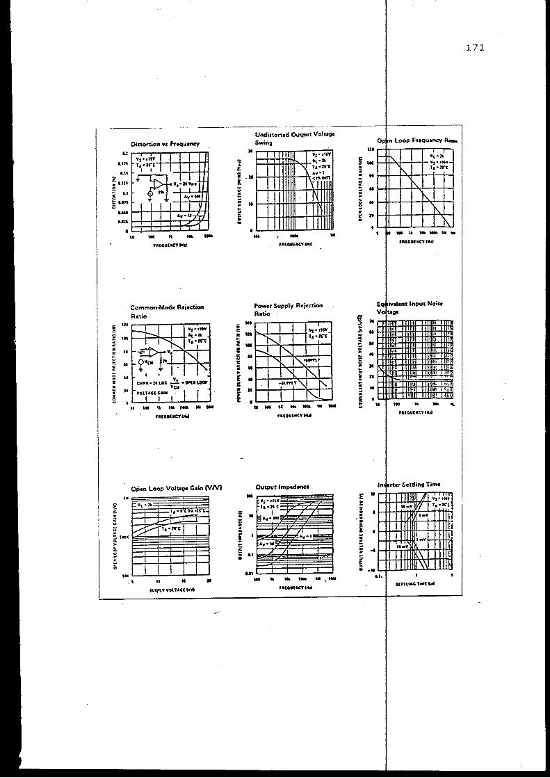
-., .. "' .. .,
~ c
" ., "' .. " ,. ~
u ..
u
t.1Jl
L!l
..... u:u
•
!211
.. o
u
"' .. Zt
'
...
~ 100(
> 0 0
"' 0
....
Distortion "' Frequency
Ys• ttiY
t•,·u;c I I
~Ye•IIYH 1
Ay•"'
I •v· u-J'rl
·~ ... -fotOUUC'tllld
Common-Mode Rejection Ratio
' ' (lilA A • II LOC ;!.!_ • trt• lOOP
~CII YUUAClCAI• I .. . .. " •• , ... ... -U£DIIt•C't Clld
OP.n loop Voltage Gain CVNI
i=•t•Zl ~· •rtto ·n·c.
I .J..--:1 ·-~···Jf"t I
t
I I I . ' II II
tllf(l Y YOlTACl It VI
... .. ~ . .. £ :; ; 0 ... ~
~ .. -
; :10
! .. "' • 0 ;:::
s " .. t ;: .. l
..
..:: w .. = r ! ~
~ .. .
•
. n
u
Undistorted Ouq,ut Voluge Swing
II Yt• I IIV ,..... 0{•1\
I ta• n"C •v•1
1\~"'0IST
I
I • ... ...
Po-r Supply Rejection Ratio
MO
ut ... .. .. It
"' •• ... - "' -fOlOVliiC'IIIUI
Output Impedance Ill
~Vs••llY la.•HC
" I
~Ay·Mt 77
y /1 ;-~ Ay•1 ....... ;;: ... / I
.... ... .. ... ·- ....... UlOIIUCYII<d
Ul
; 110 .. :
" .. ; .. ., ,. ~ 0 .. : .
21 ..
~ ,. ~ w
.. .. ~ .. ,. .. w M
0 . • ~ .. i 21 ~
; .. .. ,. • ! ..
.. ..
..... , ........ -f&lOutiiCY IIUI
lnputNoiH
HO " ... .. ratouu£YtMa•
171
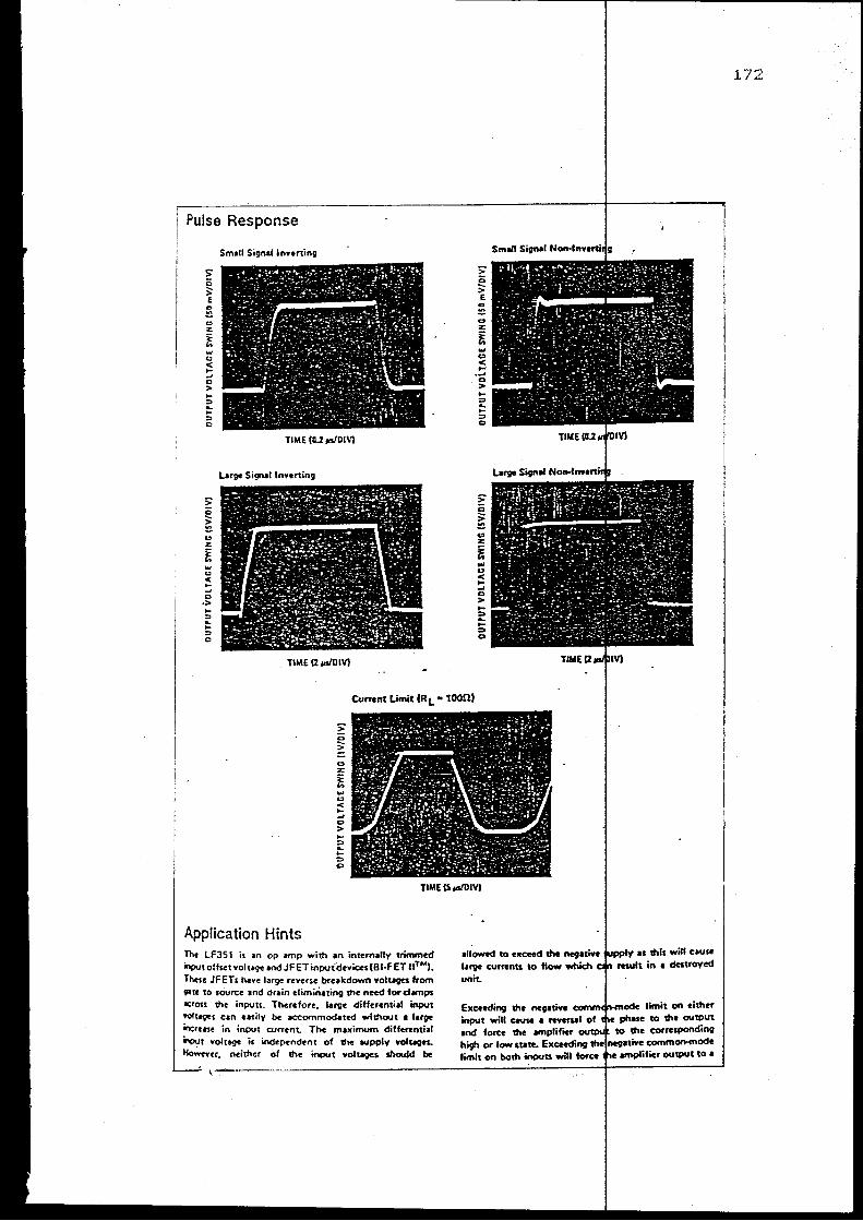
Pulse Response
> 0 > f ., .... 0 z:
~ ... " < .... oJ 0 > .... ::> ~ ::> 0
... " < .... oJ 0 ·> .... ::> .. .... ::> 0
Small Signallnnning
TIME (G.l ,.s/DIVI
La~ Sigruollnnninv
TIME (2 ,.siC IV)
> c > E
"' e
... "' < ... ·-'
D > ... ::> ... ... ::> D
Current limit IRt •100!ll
> c >
... ., < ... -' D > ... ::> ... ... ::> 0
TIME (S ,.s/DIVI
Application Hints lht LFJ51 is an op amp with an internally trimmed input offset volt19e and JFET inputdevices(Bl-FET uT""J. lhtse JFETs have large reverse breakdown volt~geS from flto to sciurce and drain eliminating the need for damps cross the inputL Therefore. large differential input tOit~s can easily be accommodated wilhout a large increase in input cu"ent. The maximum differential W\put voltage is independent of lhe supply volcages. However. neither of the input Yolt19Cs sflould be
unit.
ExcHding the nevatift u.mrndrwl~OO:If: input will cauoe a and force the amplirter high or low state. t:XCC4o<Jtl"!! ttlle~M<Jtatiore limit on both inputs will
172
output to a
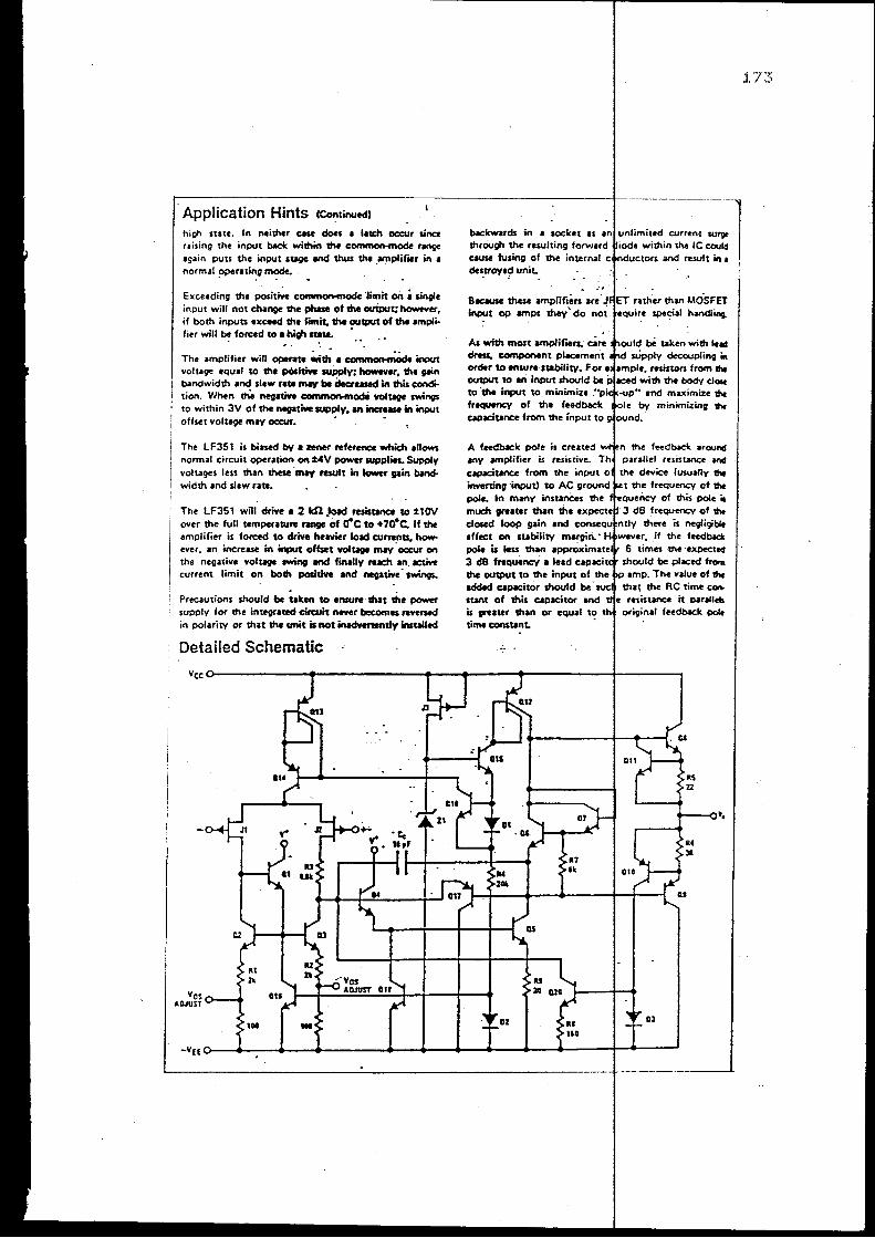
·Application Hints c~tinuedl high state. In neither cue does a latch oc:cur sina nising the input back w;thin the common-mode renge again puts the input sUge -"CC Uws the _.-nplifier in a normal ?pera ti~g mode.
Exceeding the positive common-mode "limit on a sin91c input will not cha~ the phase of the ouiput; howt¥ff, if both inpuu exceed the linlit, the ouiPUl of the ampli-fier w;u b! forced to • higltnate. •
The amplifier will operate ~th • ~e input voluge equal to the pOsftift suj:,ply; howwer, the pn bond width and slaw Ja18 m-vo be dec,eesed in this condition. When th8 negative common-mode voluge swings to within 3V of the negative supply, an inaease in input offset voltage mav oc:cur. • •
The LF351 is biased by • zener reference which allows normal circuit operation on :t.CV power supplies. Supply voltages less than these ·INV' result in klwcr pin bandwidth and slew rate.
The LF351 will drive • 2 ldl.lofd resisunc. 10 :tlOV over the full tempernure range of o•c to +7o•c. If the amplifier is forced to drive heavier load currents, however, an increase in input offset voltage may· oc:cur on the negative voiUge swing .nd finally reach an. ICtive current limit on both positive .nd negative· swings.
. . Precautions should be taken 10 ensure that the power supply for the integraced circuit never becomes reverwd in polarity or that the unit is not inadvertently installed
Detailed Schematic
backwards in a socket through the resulting cause fusing of the internal Cf'rlOIJ<:<or>
~ov•~unit.
Scause these amplifiers ~re input op amps they' do not
As with most amplif"oers. are dnss, component placement order to ensure stability. For output to ari input should be to ·tile input to minimize .•• ,,....,.~,,, ••
frequency of the feedback capacitance from the input to
A feedback pole is cruted the feedback around any amplifier is resistive. parallel resistance and
capacitanCe from the input the device {usually the inverting input) to AC the frequency of the pole. In many · neou,•nc:v of this pole i& much greater than the dB frequency of the dosed loop g.in and con .. :qu'F""Y there is negligible effect on stability n••w•rver. If the ftedboc:k pole is leu than times the -expect~<! 3 dB frequency a lead should be placed fror.. the outPUt to the input of amp. The value of the added c:apacitcir should be· tha~ the RC time c-stant of this capacitor and resistanCe it parallels is greater than or equal t~ original feedback pole
time constant.
"'-'"•
Dl
1.73
A. JUDUL
B. RUANG LINGKUP
C. LATAR BELAKANG
USULAN TUGAS AKHIR
IMPLEMENT ASI
TMS32010 UNTUK
MENGGUNAKAN MOTOR DC
- Mikroprosesor
R SINYAL
NGATURAN
DIGITAL
POSISI
- Pengolahan Sinyal igital
- Sistem Pengaturan
Munculnya
khusus dengan kern
sangat cepat
mikroprosesor tipe u
mikroprosesor
proses yang
ingkan dengan
memungkinkan
pengaturan suatu s stem yang pada
mulanya dilakukan se ara analog dapat
diu bah menjadi s stem
digital karena car ini
pengaturan
mempunyai
beberapa kelebihan daripada
analog.
sistem
Dengan sistem
dalam hal ini
prosesor sinyal d
parameter yang
konstanta penguatan
digital
menggunakan
parameter
misalnya
diubah-ubah
hanya dengan menguba pada soft
ware (misalnya melal i input keyboard)
tanpa diperlukan pengaturan pad a
rangkaian hardware-n a.
D. TUJUAN
E. PENELAAHAN STUDI
F. LANGKAH-LANGKAH
Prosesor sinyal digital TMS32010
sebagai prosesor khu us untuk operasi
pengolahan
eksekusi
sinyal imempunyai
yang san at cepat
waktu
yaitu
sebagian besar inst uksi-instruksinya
dieksekusi dalam clock cycle.
Dengan menggunakan rosesor ini di
harapkan hasil prose akan real-time.
Mempelajari implem ntasi prosesor
sinyal digital TMS3 010 untuk peng
aturan posisi dengan menggunakan motor
DC.
Mempelajari sifa -sifat dan cara
kerja prosesor TM 32010, meliputi
arsitektur internal, organisasi hard
ware, bahasa assemly dan teknik-teknik
interfacing.
Mempelajari ap ikasi prosesor
sinyal digital TMS32 10 sebagai peng
atur proses.
1. Studi literatur, yaitu melakukan
seperti telah dis di atas.
2. Perencanaan hard
3. Realisasi alat.
4. Uji peralatan dan erbaikan.
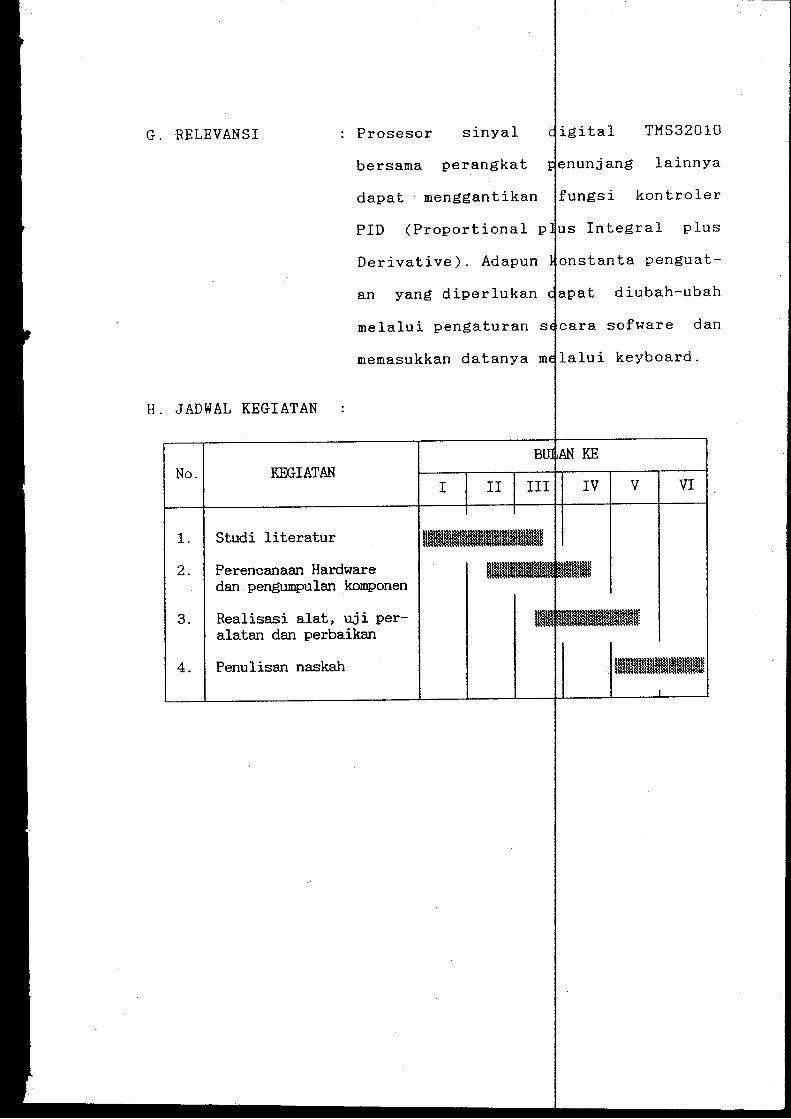
G. RELEVANSI Prosesor sinyal igital TMS32010
bersama perangkat enunjang lainnya
dapat menggantikan kontroler
PID (Proportional p s Integral plus
Derivative). Adapun onstanta penguat-
an yang diperlukan diubah-ubah
melalui pengaturan s sofware dan
memasukkan datanya m lalui keyboard.
H. JADWAL KEGIATAN
No. KEGIATAN
1. Studi literatur
2. Perencanaan Hardware dan pengumpulan komponen
3. Realisasi alat, uj i peralatan dan perbaikan
4. Penulisan naskah
I II III IV v VI
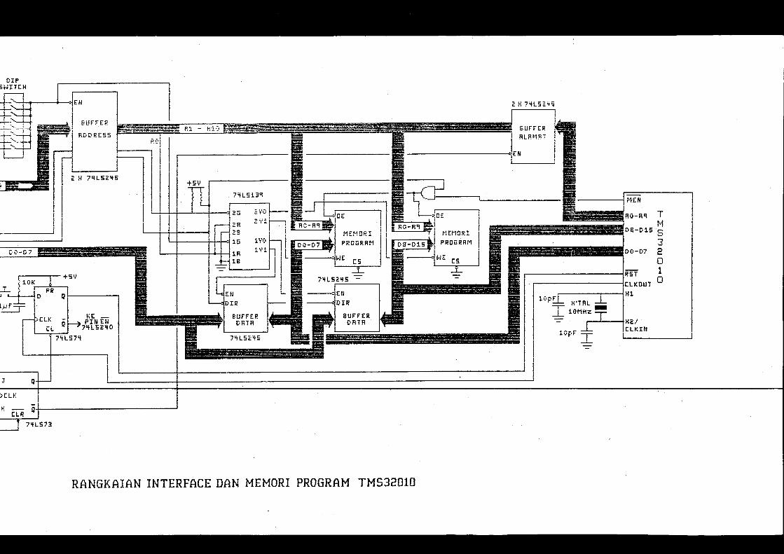
-- ! ' I -iEH
T
_j. • .i.F'
BUFFER .
Rr•DREss ...... Rl - RlO !~MFF
2 H 7'+L52'15
r-------.-- + 5 iJ
I;!!-. ------,
CL I l7'tL57'+
HI 2'+0
~--I J Q
·,eLK
K CLR
7'1L573
RANGKAIAN INTERFACE DAN MEMORI PROGRAM TMS32010
2 K 7'fL52-tS
·~:-~~~=~~ ~RO-R'I - - ~;~ -;::~~-=-==~~~"'~:~;:;s~-=-_::::-==-~=-'-
3 -:7 --~"'"::;-:;._::,:C ~. ~,_ t--::-_c'"> ---: =-=-- · D 0- 07 2
0 1
r-------------------iriKOUT 0
I I IH2/
lOpF I lt:LKitl
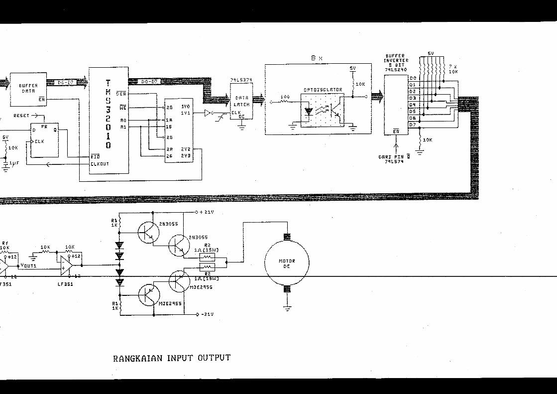
T ~*- ~:._,.- .--~~-=!:.. -·: ;s;_~=::: ~=---=-~~.=::..
u-:-: DE ~J
Efl ~ -.J
3 WE I I
r------1->t 2 r; 1 \' 0 1V1
2 RO
0 R1
Si.'
~ iOK
'
- .;::u· ' •
LJ II-~ - 1 (ro
CLKOUT ... I.?-J-!' -=
0 + 21\.1
l ~ -.u':lr.Ss I u 5 ~ _ ""'"--· I iii f ( 1.,.. ) --t.. ~H30SS !\1'~ ' // ,-·· .,)~ fi!2
, ''-J/ / ~~ 1l'L [15WJ -~:.t_,. .... _ Rf OK 10~; lOK .M·~ ....... ----t-:-.... .,"----, -. ·r· +12 1 -:f""""' 1 I' ... ~ +12 1 '..t l ]---.1 I ·:=-1 Voun+ . ) • • A - !-/
351
Ri 1K
L-----t-------'---ov -21 V
7~LS37if
RA.NGKA.IAN INPUT OUTPUT
8 ;-:
Y-l i ' ., (!!.-"
·~_1~110 I ~p~~I~~L~~O·;r-R I s ~ ") • ~ ·I .1' ~ • ·.-~-y="'K-
~;_...: ...... ,.·
. . . -=
~ .1~ ,,
/ \ ; \
( MOTOR ) 1
DC
\ -
"'-.. / r -=
BUF'F'ER INVERTER
s iiiT 7'1L52'10
SV
mnn 7 ;: 10K


